Substrate plating jig

A substrate and fixture technology, which is applied in the fields of electrical components, electrolysis process, semiconductor/solid-state device manufacturing, etc., can solve the problems of large number of parts, complicated replacement of seals, and high cost, and achieve uniform plating liquid flow and easy replacement operations Effect

Inactive Publication Date: 2015-07-15
JCU CORP
View PDF9 Cites 5 Cited by
  • Summary
  • Abstract
  • Description
  • Claims
  • Application Information

AI Technical Summary

Problems solved by technology

[0005] However, in the plating jig disclosed in Patent Document 1, the holding part itself has a thickness so that a part of the guide pins for positioning the substrate can be buried, and therefore, the uniformity of plating may be affected.
In addition, the number of parts is large, the cost is high, and the replacement work of the seal is also complicated.

Method used


Image

  • Substrate plating jig
  • Substrate plating jig
  • Substrate plating jig

Examples


Embodiment Construction

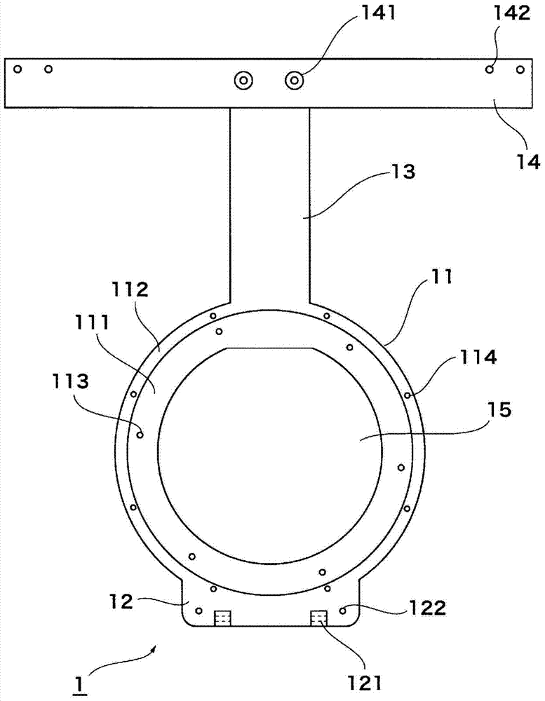
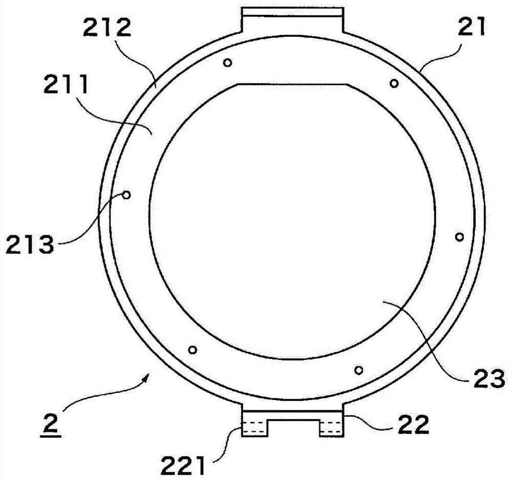
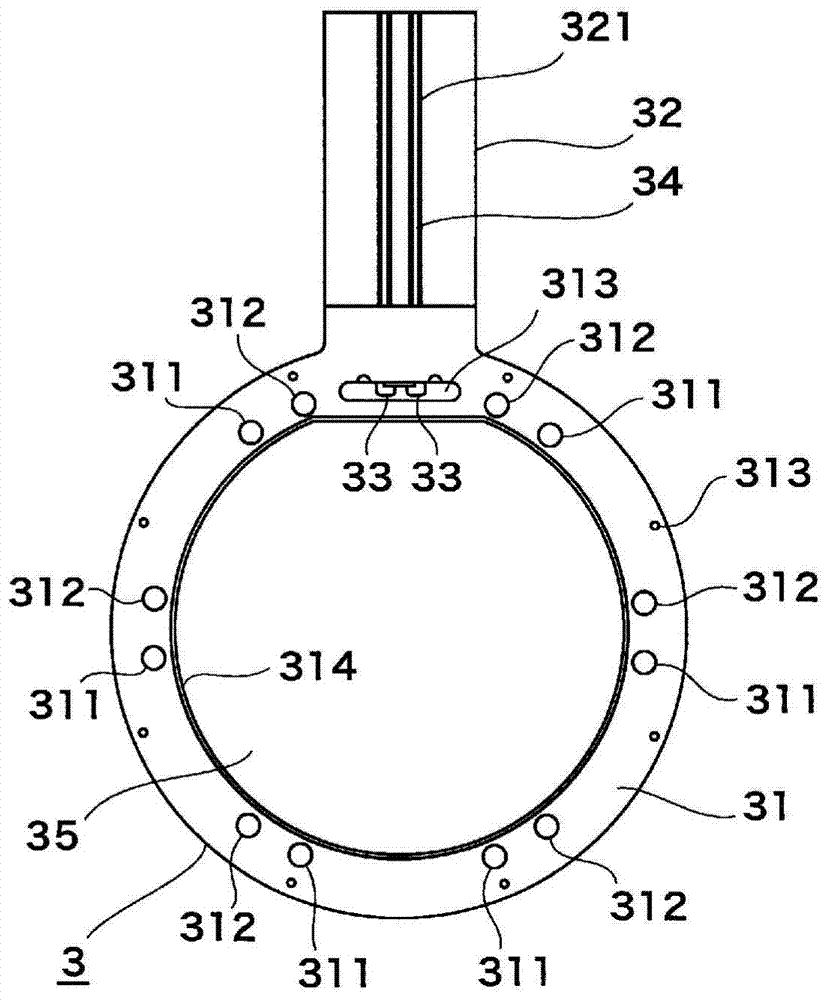
[0022] Hereinafter, embodiment of the plating jig of this invention is demonstrated concretely based on drawing. In addition, the present invention is not limited to these embodiments.

[0023] figure 1 It is the front view of the base part of the plating jig of the present invention, figure 2 It is the front view of the cover part of the plating jig of the present invention, image 3 It is a front view of the central part of the plating jig of the present invention, Figure 4 It is the front view of the clamp part of the plating jig of the present invention, Figure 5 It is a front view of the gasket 5 in a state where the energization ring 6 is arranged inside, Image 6 It is a front view of the state where the clamp part 4 and the cover part 2 are opened after the plating jig of the present invention is assembled, Figure 7 It is a partially enlarged cross-sectional view of a state in which the substrate W is held by the plating jig of the present invention.

[0024]...


PUM


Abstract

The purpose of the present invention is to provide a plating jig, which is capable of forming metal plating films at the same time on both the surfaces of a semiconductor wafer by performing plating one time, and which has a simple configuration with a thinner holding section. This plating jig is provided with: a base section and a cover section, which are formed such that the sections can hold a substrate to be plated; and a center section, which is sandwiched between the base section and the cover section, and which aligns the substrate to be plated. The plating jig is characterized in that: each of the base section, the cover section, and the center section has an annular portion having an opening at the center; to each of the facing surfaces of the base section annular portion and the cover section annular portion, a seal packing having a conductive ring disposed thereon is attached; the substrate to be plated is disposed in the opening of the center section; and the substrate to be plated is sandwiched from both the front and rear surfaces by means of the seal packing attached to each of the cover section and the center section.

Description

technical field [0001] The present invention relates to a plating jig used in the plating process of a substrate, and more particularly to a plating jig for forming fine wiring grooves and holes on a surface to be plated, such as a semiconductor wafer, and forming a plating jig in a resist opening. A plating jig that forms bumps (protruding electrodes) that electrically connect a semiconductor chip to a substrate on the surface of a semiconductor wafer to be coated or coated. Background technique [0002] A conventional general plating jig has a holding member that seals the outer peripheral end surface and the back surface of a substrate such as a semiconductor wafer and exposes and holds the surface (surface to be plated). The holding member is immersed in a plating solution together with the substrate. To perform plating on the plated surface of the substrate. [0003] However, in the electrolytic plating method using the above-mentioned conventional plating jig, only on...

Claims


Application Information

Patent Timeline
Patent Type & Authority Applications(China)
IPC IPC(8): C25D17/06
CPCC25D17/001C25D17/06H01L21/68721
Inventor 吉冈润一郎村山隆史
Owner JCU CORP
Why Eureka
Try Eureka