Wafer alignment mark

A technology for aligning marks and wafers, applied in electrical components, electric solid-state devices, circuits, etc., can solve the problems of affecting wafer bonding accuracy, waste of resources, and reducing the effective area of ​​​​the chip, and achieve a large effective area of ​​​​the chip. Effect

Active Publication Date: 2015-06-10
WUHAN XINXIN SEMICON MFG CO LTD
View PDF5 Cites 9 Cited by
  • Summary
  • Abstract
  • Description
  • Claims
  • Application Information

AI Technical Summary

Problems solved by technology

[0003] In the current wafer-to-wafer bonding technology, the alignment marks used in the wafer bonding process generally adopt a horizontal design and are placed at the intersection of the two scribe lines of the wafer. When the scribe line width If the bonding alignment mark becomes smaller, the bonding alignment mark cannot be placed in the dicing lane, and the effective area of ​​the chip must be occupied or the size of the bonding alignment mark must be reduced. Occupying the effective area of ​​the chip will reduce the effective area of ​​the chip, thereby causing a waste of resources. Reducing the size of the bonding alignment mark will affect the bonding accuracy of the wafer, which is undesirable for those skilled in the art

Method used


Image

  • Wafer alignment mark
  • Wafer alignment mark
  • Wafer alignment mark

Examples


Embodiment Construction

[0017] The present invention will be further described below in conjunction with the accompanying drawings and specific embodiments, but not as a limitation of the present invention.

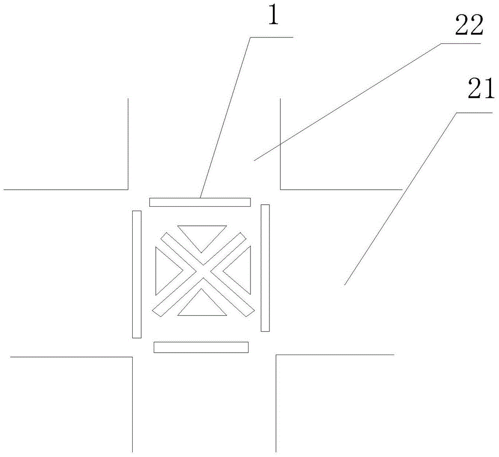
[0018] The invention discloses a wafer alignment mark. The alignment mark can be applied in the bonding process of wafers. The wafer is provided with cutting lines intersecting each other, and a tip pattern is provided on the crossing area of ​​the cutting lines. alignment marks, and the tip pattern extends into non-intersecting areas of the dicing lanes.

[0019] In a preferred embodiment of the present invention, the above-mentioned cutting lines may include horizontal cutting lines and vertical cutting lines perpendicular to each other.

[0020] On this basis, further, the angle formed between the alignment mark and the horizontal cutting line is not 0°, preferably, the value range of the angle between the alignment mark and the horizontal cutting line is 30°-60°( For example 30°, 45°, 50° o...


PUM


Abstract

The invention relates to the semiconductor manufacture technical field, and in particular relates to an alignment mark applied to the wafer bonding process; the alignment mark is arranged on the intersection region of the wafer cutting way, the cutting-edge graphics of the alignment mark extends into the non-intersection region of the wafer cutting way, so that the alignment mark is suitable for the wafer cutting way with smaller size while the size of the alignment mark is not reduced and the wafer bonding precision is not influenced, and larger chip effective area can be achieved.

Description

technical field [0001] The invention relates to the technical field of semiconductor manufacturing, in particular to an alignment mark applied to a wafer bonding process. Background technique [0002] In 3D-IC technology, the bonding process between wafers is a very critical technology. The quality of the bonding process between two wafers determines the success of the entire process. Among them, for bonding Alignment marks play a crucial role in the process. [0003] In the current wafer-to-wafer bonding technology, the alignment marks used in the wafer bonding process generally adopt a horizontal design and are placed at the intersection of the two scribe lines of the wafer. When the scribe line width If the bonding alignment mark becomes smaller, the bonding alignment mark cannot be placed in the dicing lane, and the effective area of ​​the chip must be occupied or the size of the bonding alignment mark must be reduced. Occupying the effective area of ​​the chip will red...

Claims


Application Information

Patent Timeline
Patent Type & Authority Applications(China)
IPC IPC(8): H01L23/544
Inventor 王佳刘天建陈海平胡杏
Owner WUHAN XINXIN SEMICON MFG CO LTD
Why Eureka
Try Eureka