A Microstrip Patch Antenna Based on Photonic Crystal Structure
A microstrip patch antenna, photonic crystal technology, applied in the directions of antenna coupling, radiating element structure, etc., can solve the problems of narrow operating frequency band, low radiation efficiency, low gain of antenna microstrip antenna, etc. The effect of solving low gain and realizing miniaturization
- Summary
- Abstract
- Description
- Claims
- Application Information
AI Technical Summary
Problems solved by technology
Method used
Image
Examples
Embodiment Construction
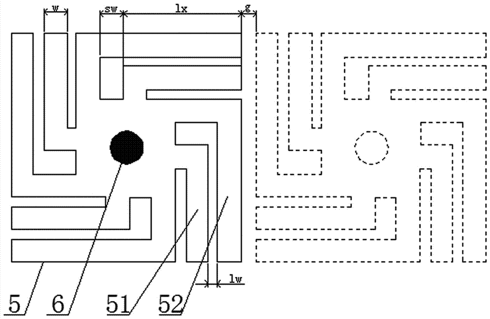
[0019] Such as Figure 1 to Figure 3 As shown, a microstrip patch antenna based on a photonic crystal structure includes a dielectric substrate 1, a metal ground layer 4 is provided on the back of the dielectric substrate 1, and a radiation branch 2 is provided in the center of the front of the dielectric substrate 1, and the radiation branch 2 is a mirror image Symmetrical four-helix structure, surrounded by a photonic crystal band gap layer, the photonic crystal band gap layer is set flush with the radiation branch 2, and the photonic crystal band gap layer consists of 2 rows (columns), a total of 48 metal patches arranged periodically 5, the metal patch 5 includes a central part, the center of the central part is connected to the metal ground layer 4 through a conductive via 6, and a plurality of L-shaped first metal microstrip lines 51 and The second metal microstrip line 52 and the metal ground layer 4 are connected to the radiation stub 2 through the feeding port 3 , and...
PUM
 Abstract
Description
Claims
Application Information
 - R&D
- Intellectual Property
- Life Sciences
- Materials
- Tech Scout
- Unparalleled Data Quality
- Higher Quality Content
- 60% Fewer Hallucinations
Browse by: Latest US Patents, China's latest patents, Technical Efficacy Thesaurus, Application Domain, Technology Topic, Popular Technical Reports.
© 2025 PatSnap. All rights reserved.Legal|Privacy policy|Modern Slavery Act Transparency Statement|Sitemap|About US| Contact US: help@patsnap.com


