LED (Light Emitting Diode) light source, backlight module and liquid crystal display device

An LED light source and light technology, applied in the field of optics, can solve the problems of increasing product cost, inability to effectively adjust the luminous angle of the LED light source, poor optics, etc., to achieve the effect of increasing the luminous angle and improving the utilization efficiency of the light source

Inactive Publication Date: 2015-04-29
SHANGHAI TIANMA MICRO ELECTRONICS CO LTD +1
View PDF8 Cites 11 Cited by
  • Summary
  • Abstract
  • Description
  • Claims
  • Application Information

AI Technical Summary

Problems solved by technology

When the LED light source is applied to the side-emitting backlight module, it is a point light source, and the light-emitting state is fan-shaped emission. When the light-emitting angle is small, it often causes the optical defect phenomenon of "firefly" (uneven light mixing), which affects the display effect.
In addition, when applied to the backlight of a display device in a direct-lit backlight module, if the light emitting angle of the LED light source is small, it is necessary to increase the number of LED light sources in the module, which increases the product cost
[0005] see Figure 1b , because the LED light source is a line light source, when it is applied to a backlight source, it needs to be converted into a surface light source by using the light guide plate 13, but when the LED light source is placed on the side of the light guide plate, the thickness d of the light guide plate is small, and the LED light source in the light guide The light emitting angle β in the thickness direction of the light plate is too large, and the plane covered by it is far beyond the side of the light guide plate, so the light beyond the thickness of the side of the light guide plate, that is Figure 1b The light in areas A and C is wasted, and the utilization efficiency is not high
Therefore, the lighting angle of the LED light source cannot be effectively adjusted in the prior art

Method used


Image

  • LED (Light Emitting Diode) light source, backlight module and liquid crystal display device
  • LED (Light Emitting Diode) light source, backlight module and liquid crystal display device
  • LED (Light Emitting Diode) light source, backlight module and liquid crystal display device

Examples


Embodiment Construction

[0033] The present invention will be further described in detail below in conjunction with the accompanying drawings and embodiments. It should be understood that the specific embodiments described here are only used to explain the present invention, but not to limit the present invention. In addition, it should be noted that, for the convenience of description, only some structures related to the present invention are shown in the drawings but not all structures.

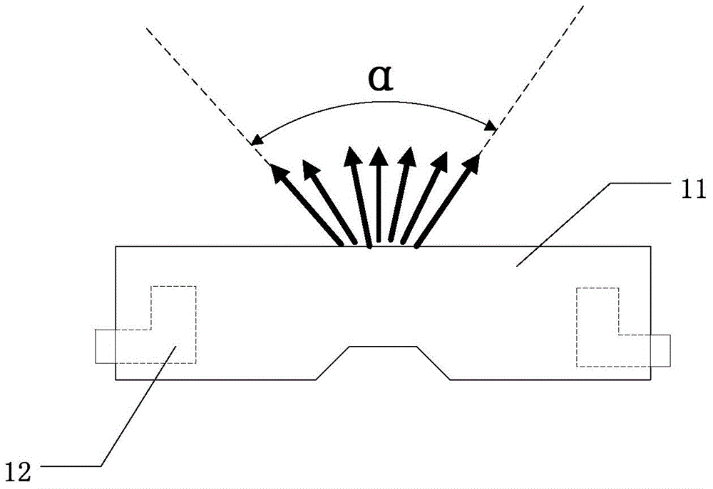
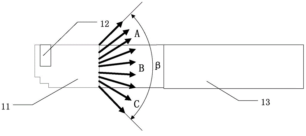
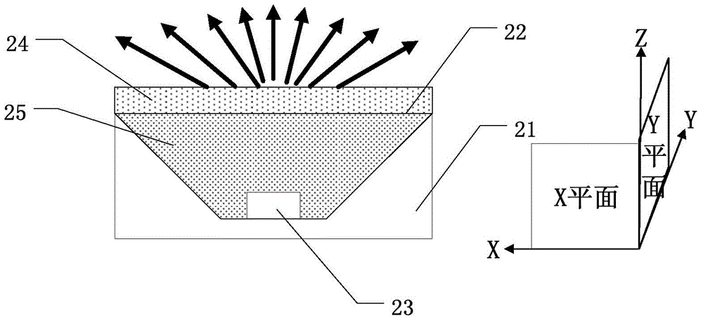
[0034] An embodiment of the present invention provides an LED light source. figure 2 It is a schematic cross-sectional structure diagram of an LED light source provided by an embodiment of the present invention. Such as figure 2 As shown, the LED light source includes: a casing 21, the casing has a light outlet 22; an LED chip 23 is arranged in the casing 21, and the light-emitting surface of the LED chip 23 faces the light outlet of the casing. 22. The light adjustment layer 24 is located at the light outlet ...


PUM

PropertyMeasurementUnit
radiusaaaaaaaaaa

Abstract

The invention discloses LED (Light Emitting Diode) light sources, a backlight module and a liquid crystal display device. Every LED light source comprises a housing, an LED wafer and a light adjustment layer, wherein the housing comprises a light outlet, the LED wafer is arranged in the housing, the light emitting surface of the LED wafer is towards the light outlet of the housing, and the light adjustment layer is located at the position of the light outlet of the housing; the backlight module comprises the LED light sources and a light guide plate, wherein the LED light sources are located in the same plane to form a backlight source array, the plane of the backlight source array is located under the light guide plate or the LED light sources are located on the lateral side of the light guide plate and located in the same plane, and the plane of the LED light sources is parallel to the lateral side of the light guide plate; the liquid crystal display device comprises a liquid crystal display panel and the backlight module. According to the LED light sources, the backlight module and the liquid crystal display device, the light emitting angle of the LED light sources can be effectively adjusted.

Description

technical field [0001] The invention relates to the field of optics, in particular to an LED light source, a backlight module and a liquid crystal display device. Background technique [0002] Semiconductor solid-state lighting is one of the most promising new technologies in the 21st century, and its core is high-power LED. In recent years, with the advancement of semiconductor material growth technology and device packaging technology, the luminous efficiency and reliability of high-power LED devices have been greatly improved. The application range of LED is also becoming wider and wider, among which the application of LED in lighting and display panels is very rapid. Whether it is applied to lighting or as a backlight source for a display panel, it is of great value to manufacture an LED package device with a larger luminous angle. [0003] In the prior art, the power-type LED generally determines the light-emitting angle of the LED by the cup depth of the bracket, the...

Claims


Application Information

Patent Timeline
Patent Type & Authority Applications(China)
IPC IPC(8): G02F1/13357H01L33/58F21V9/00F21V5/00G02B5/02G02B5/04
CPCF21V5/005F21V9/00G02B5/0231G02B5/045G02F1/133603G02F1/133606G02F1/133607H01L33/58G02B5/0242G02B6/0025G02B6/0068G02B6/0073H01L33/507H01L2933/0091
Inventor 尧璐
Owner SHANGHAI TIANMA MICRO ELECTRONICS CO LTD
Why Eureka
Try Eureka