Double-side polishing method of 12-inch silicon wafer

A double-sided polishing, silicon wafer technology, applied in the polishing field, can solve problems such as uneven wear of polishing pads, and achieve the effects of improving the amount of wear, slowing down the glazing speed, and reducing the number of dressing times.

Inactive Publication Date: 2015-04-29
GRINM SEMICONDUCTOR MATERIALS CO LTD
View PDF5 Cites 2 Cited by
  • Summary
  • Abstract
  • Description
  • Claims
  • Application Information

AI Technical Summary

Problems solved by technology

[0006] The object of the present invention is to provide a double-sided polishing method for a 12-inch silicon wafer, to improve the uneven wear of the polishing pad, thereby reducing the inhomogeneity of the silicon wafer and between the sheets, and increasing the service life of the polishing pad. Increased stability of the polishing process

Method used


Image

  • Double-side polishing method of 12-inch silicon wafer
  • Double-side polishing method of 12-inch silicon wafer
  • Double-side polishing method of 12-inch silicon wafer

Examples


Embodiment 1

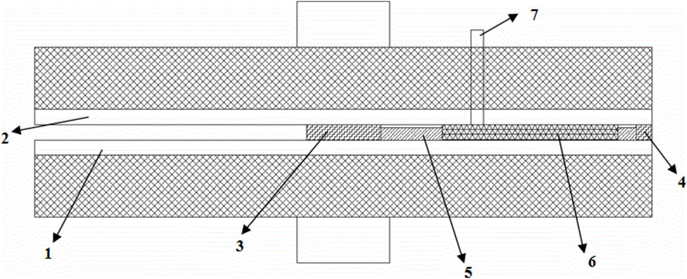
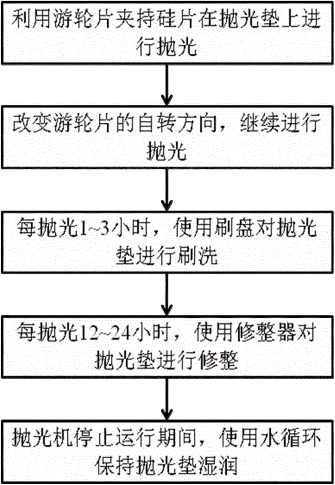
[0024] Choose 400 pieces of 12-inch P(100) silicon wafers grown by the Czochralski method, divided into four groups A, B, C, and D, with 100 pieces in each group. After single-side grinding, the thickness is about 800 μm, all in SPEEDFAM20B Polishing was carried out on a double-sided polishing machine, 5 silicon wafers were polished per plate, the polishing pad was SUBA800, and the polishing removal amount was 25 μm (polishing time was about 50 minutes).

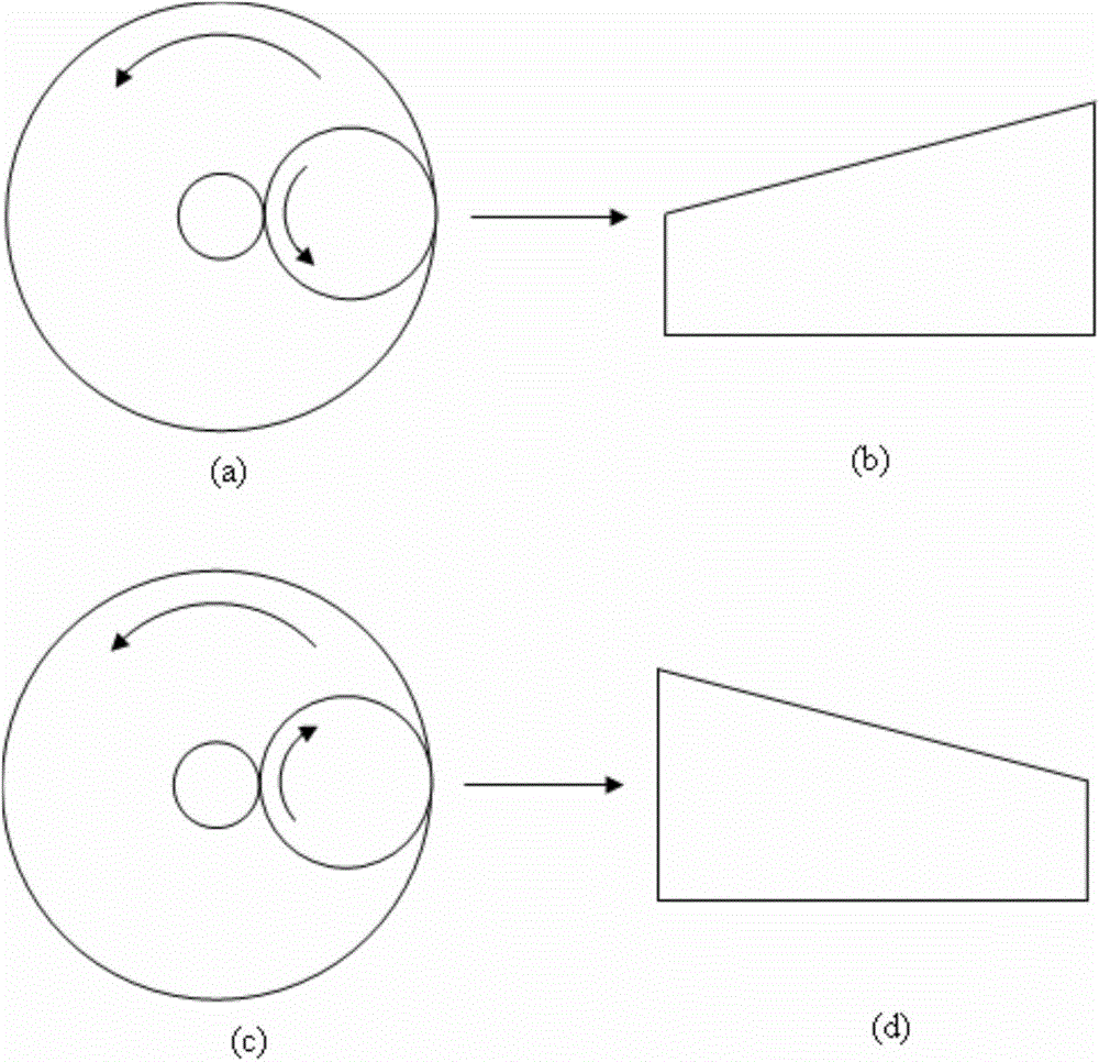
[0025] For group A, the conventional method is used for polishing, that is, the relative movement direction of the cruiser plate and the polishing pad remains unchanged, and the polishing is carried out continuously without brushing or repairing between the discs; for group B, the conventional method is used for polishing. After polishing a silicon wafer, use a brush to scrub the polishing pad without repairing the disk; for group C, use the conventional method for polishing. After polishing a silicon wafer, use a brush to sc...

Embodiment 2

[0029] The two polishing cloths E and F were both polished on both sides normally using the scheme of Group D in Example 1. When the polishing machine is stopped, do not spray water on the surface of the polishing cloth E, and let it dry naturally; for the polishing cloth F, use water circulation to keep the surface of the polishing cloth wet. Ultimately, Cloth E had a service life of 60 hours, and Cloth F had a service life of 80 hours. It can be seen that when the polishing machine is stopped, pure water circulates through the polishing liquid pipeline to keep the surface of the polishing cloth moist and prolong the service life of the polishing cloth.


PUM


Abstract

The invention provides a double-side polishing method of a 12-inch silicon wafer. The method includes the steps of firstly, placing the silicon wafer in the carrier of a polishing machine, allowing he silicon wafer to move relative to an upper polishing pad and a lower polishing pad under the drive of a sun gear and an outer gear ring, and alternately changing the rotation direction of the carrier so as to polish the surface of the silicon wafer; using a brush plate to brush the upper polishing pad and the lower polishing pad after the silicon water is polished for every 1-3 hours, wherein purified water is sprayed to the polishing pads during the brushing; thirdly, using a diamond trimmer to trim the upper and lower polishing pads after the silicon water is polished for every 12-24 hours, wherein purified water is sprayed to the polishing pads during the trimming. The method has the advantages that the phenomenon that the abrasion loss at the center of the polishing pads is different from that at the edge of the polishing pads can be improved effectively, residual impurities on the surfaces of the polishing pads can be removed effectively by the brush plate, glazing speed of the polishing pads is slowed, heterogeneity in the silicon wafer and between silicon wafers can be lowered, the trimming times of the polishing pads are reduced, polishing stability is increased, and production cost is lowered.

Description

technical field [0001] The invention relates to a double-sided polishing method for a 12-inch silicon wafer, in particular to a polishing method for improving polishing stability, reducing intra-chip and inter-chip non-uniformity, and prolonging the service life of polishing cloths. Background technique [0002] At present, in the semiconductor industry, 12-inch silicon wafers have become the mainstream, and silicon wafers with a diameter of 18 inches are still in the development stage. [0003] Due to the lower economic cost and higher flatness of the products produced by double-side polishing, it has become the main polishing process for large-diameter silicon wafers. Such as figure 1 Shown is a cross-sectional view of a double-sided polishing machine. The double-sided polishing machine mainly includes a lower polishing pad 1, an upper polishing pad 2, a sun gear 3, an outer ring gear 4, and a cruiser piece 5 located between the sun gear 3 and the outer gear ring 4. Duri...

Claims


Application Information

Patent Timeline
Patent Type & Authority Applications(China)
IPC IPC(8): B24B29/02B24B57/02B24B53/017
CPCB24B37/08B24B29/02B24B53/017B24B57/02
Inventor 王永涛闫志瑞库黎明冯泉林葛钟
Owner GRINM SEMICONDUCTOR MATERIALS CO LTD
Why Eureka
Try Eureka