Preparation method of field cut-off type insulated gate bipolar transistor

A technology of bipolar transistors and insulated gates, which is applied in the direction of transistors, semiconductor/solid-state device manufacturing, semiconductor devices, etc., and can solve problems such as easy scratches on wafers

Active Publication Date: 2015-04-15
CSMC TECH FAB2 CO LTD
View PDF4 Cites 0 Cited by
  • Summary
  • Abstract
  • Description
  • Claims
  • Application Information

AI Technical Summary

Problems solved by technology

[0004] Based on this, in order to solve the problem that the front side of the wafer (wafer) is easily scratched during the manufacturing process of the traditional insulated gate bipolar transistor, it is necessary to provide a method for preparing a field stop type insulated gate bipolar transistor

Method used


Image

  • Preparation method of field cut-off type insulated gate bipolar transistor
  • Preparation method of field cut-off type insulated gate bipolar transistor
  • Preparation method of field cut-off type insulated gate bipolar transistor

Examples


Embodiment Construction

[0018] In order to make the objects, features and advantages of the present invention more comprehensible, specific implementations of the present invention will be described in detail below in conjunction with the accompanying drawings.

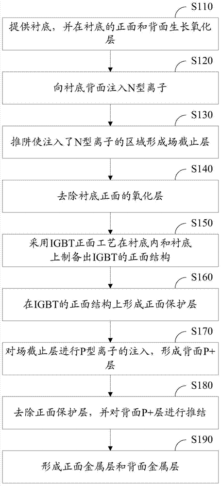
[0019] figure 1 It is a flowchart of a method for preparing a field-stop type insulated gate bipolar transistor according to an embodiment, including the following steps:

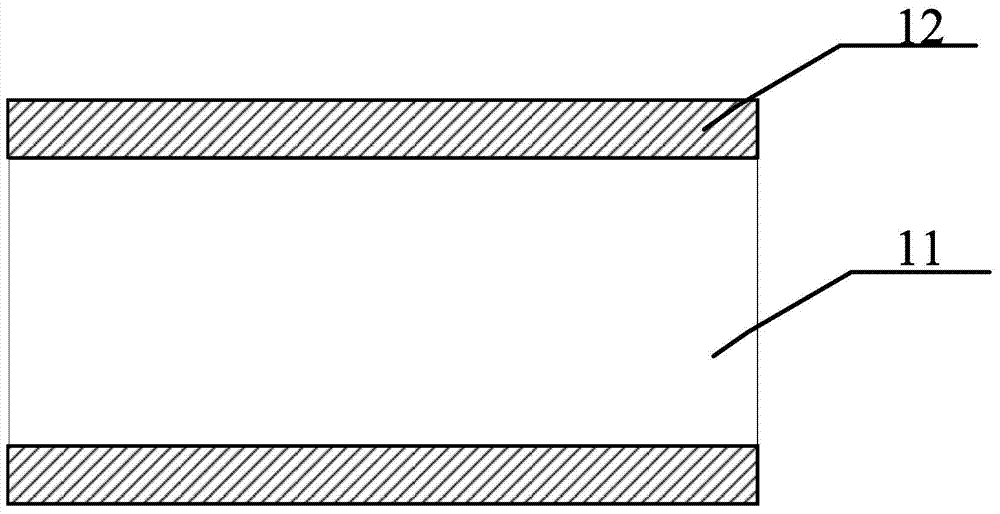
[0020] S110, providing a substrate, and growing an oxide layer on the front side and the back side of the substrate.

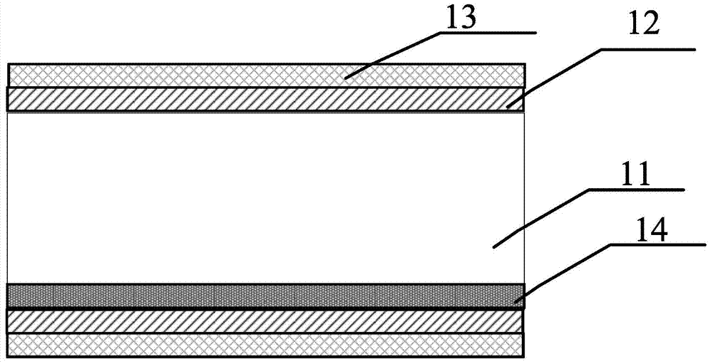
[0021] In this embodiment, a Raw Wafer with a thickness of about 400 microns is used as the substrate 11, and the first oxide layer 12 is grown on the front and back sides of the substrate 11, referring to Figure 2A . It can be understood that in this embodiment, due to process limitations, oxide layers are formed on the front and back sides at the same time. In the drawings, the oxide layers on the front and back sides of the substrate 11 are collecti...


PUM

PropertyMeasurementUnit
Thicknessaaaaaaaaaa

Abstract

A method for preparing a field stop insulated gate bipolar transistor (IGBT) comprises the following steps: providing a substrate (11), and growing a first oxidizing layer (12) on the front and the back of the substrate (11); internally injecting N-type ions from the back of the substrate (11); performing trap pushing on the substrate (11), to make an area injected with N-type ions form a field stop layer (14); removing the first oxidizing layer (12) on the front of the substrate (11); preparing a front structure of the IGBT in the substrate (11) and on the front of the substrate (11) by using an IGBT front process; forming a front protection layer on the front structure; injecting P-type ions into the field stop layer, to form a back P+ layer (23); removing the front protection layer, and performing knotting pushing on the back P+ layer (23); and forming a front metal layer (27) on one of the front structure and the back P+ layer (23), and forming a back metal layer (28) on the other of the front structure and the back P+ layer (23). By growing the first oxidizing layer (12) on the front and forming the front protection layer after the front structure is formed, the front of a wafer can be protected, and the wafer is not easy to be scratched in a manufacturing process.

Description

technical field [0001] The invention relates to a manufacturing method of a semiconductor device, in particular to a manufacturing method of a field-stop insulated gate bipolar transistor. Background technique [0002] Due to the conductance modulation effect, an insulated gate bipolar transistor (Insulated Gate Bipolar Transistor, IGBT for short) has a lower on-resistance than a DMOS. So far, IGBT mainly has three structures: punch-through PT-IGBT, non-punch-through NPT-IGBT and field-stop FS-IGBT. The main differences between the three are different substrate PN junction structures and different drift region thicknesses. . Compared with PT-IGBT and NPT-IGBT, the thickness of FS-IGBT is the thinnest, but the expensive sheet equipment, complicated process and high fragmentation rate seriously limit the performance of FS-IGBT (especially low-voltage IGBT). constantly improving. [0003] On the other hand, for traditional FS-IGBTs, after the FS layer is completed on the bac...

Claims


Application Information

Patent Timeline
IPC IPC(8): H01L21/331
CPCH01L29/7395H01L29/66333
Inventor 邓小社王根毅钟圣荣周东飞
Owner CSMC TECH FAB2 CO LTD
Why Eureka
Try Eureka