
Pixel structure, display method of pixel structure and display device

A pixel structure and sub-pixel technology, applied in static indicators, optics, instruments, etc., can solve problems such as difficulty in ensuring sub-pixel aperture ratio, affecting product life, brightness, and difficulty in realizing high resolution, so as to improve pixel aperture ratio , reduce power consumption, improve the effect of pixel resolution

Active Publication Date: 2015-03-25
BOE TECH GRP CO LTD
View PDF5 Cites 77 Cited by
  • Summary
  • Abstract
  • Description
  • Claims
  • Application Information

AI Technical Summary

Problems solved by technology

Among them, FMM generally has the limitation of the minimum opening, and the sub-pixels of different colors in the evaporation process are limited by the opening pitch. Therefore, the preparation of AMOLED is inevitably limited by the FMM opening and the precision of the evaporation process. It is difficult to achieve high resolution. If a higher resolution is required, it is difficult to ensure the aperture ratio of the sub-pixels, making it difficult to achieve high resolution, and even affect the product's lifespan, brightness and other characteristics

Method used


Image

  • Pixel structure, display method of pixel structure and display device
  • Pixel structure, display method of pixel structure and display device
  • Pixel structure, display method of pixel structure and display device

Examples


Embodiment 1

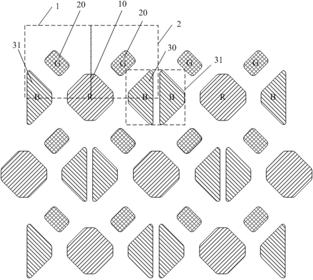
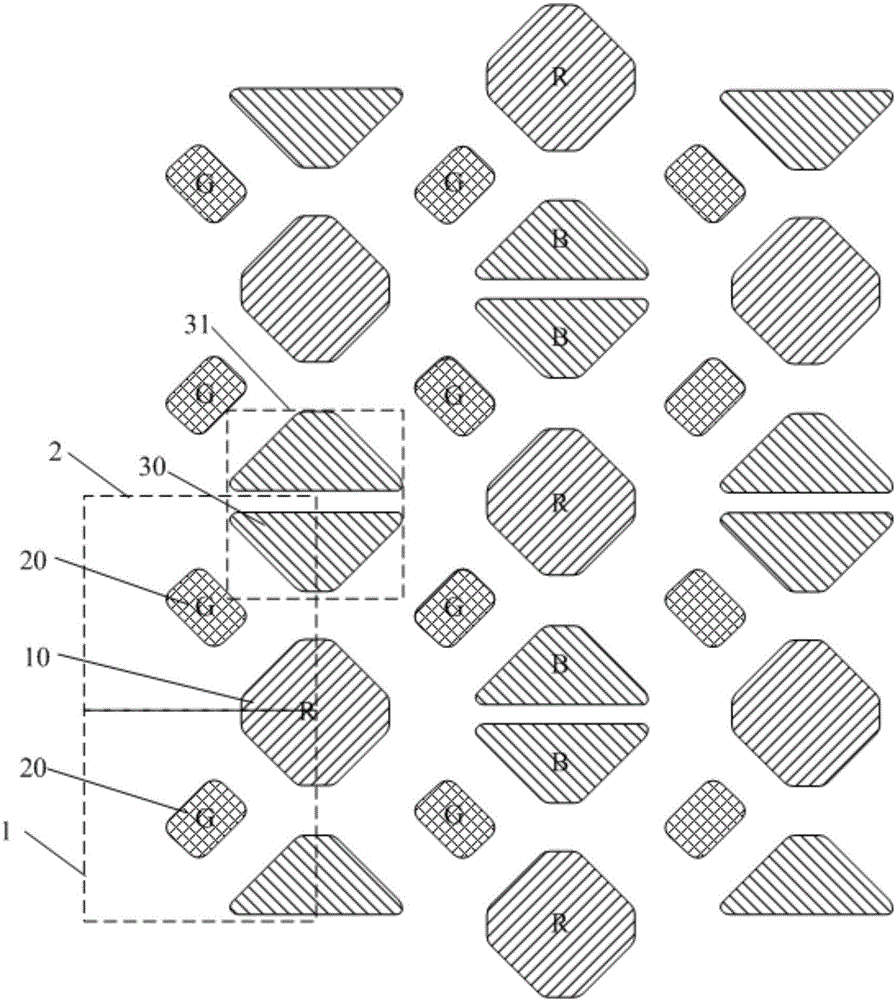
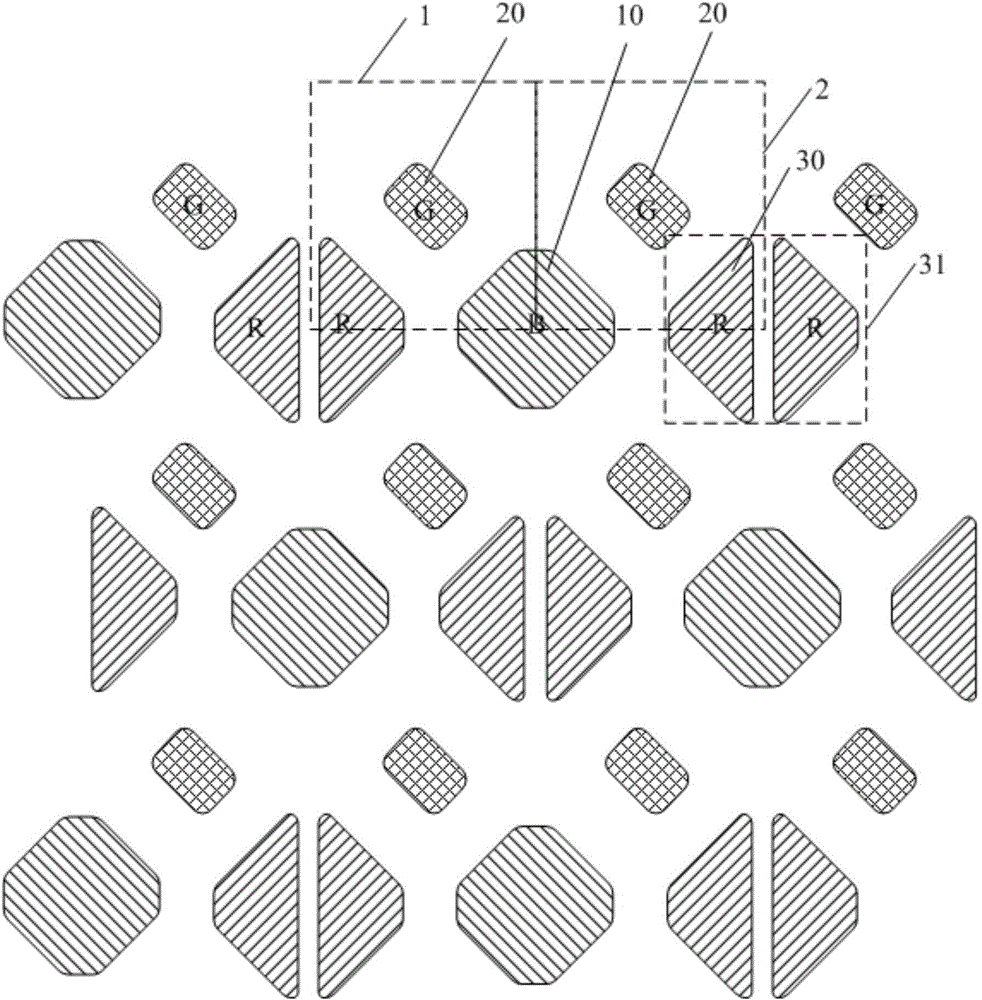
[0055] This embodiment provides a pixel structure, such as figure 1 As shown, the pixel structure includes a first sub-pixel 10, a second sub-pixel 20, and a third sub-pixel 30, wherein two adjacent third sub-pixels 30 oppositely arranged form a third sub-pixel group 31, and the second The two sub-pixels 20 are arranged in the row direction to form the second sub-pixel row, the first sub-pixel 10 and the third sub-pixel group 31 are alternately arranged in the row direction, the second sub-pixel row is the same as the first sub-pixel 10 and the third sub-pixel group The rows formed by 31 are arranged alternately. Wherein, the two third sub-pixels 30 adjacent to each other refer to: two third sub-pixels 30 that are closest in distance and have approximately the same size and shape or are mirror-symmetrical are opposite along the axis between them. It is provided that, if the two third sub-pixels 30 move relatively toward the axis respectively, the two third sub-pixels 30 can b...

Embodiment 2

[0092] This embodiment provides a display method corresponding to the pixel structure in Embodiment 1. In this pixel structure, adjacent pixel units share the first sub-pixel for display, realizing display of five sub-pixels instead of six sub-pixels, so that adjacent pixel units can display pixel display information of three display colors.

[0093] Specifically, in the pixel structure, the second sub-pixel 20 and a third sub-pixel 30 and a first sub-pixel 10 located in the adjacent row and adjacent to it form a pixel unit, except for odd-numbered or even-numbered rows The first pixel unit and / or the last pixel unit, each pixel unit shares the first sub-pixel 10 with a pixel unit located in the same row and adjacent to it; or, the second sub-pixel 20 and the adjacent pixel unit A third sub-pixel 30 and a first sub-pixel 10 adjacent to it in an adjacent column form a pixel unit, except for the first pixel unit and / or the last pixel unit in an odd or even column, each pixel uni...

Embodiment 3

[0109] This embodiment provides a display device, which adopts the pixel structure in Embodiment 1 and the display method of the pixel structure in Embodiment 2.

[0110] The display device can be any product or component with a display function such as a liquid crystal panel, an electronic paper, an OLED panel, a mobile phone, a tablet computer, a television, a monitor, a notebook computer, a digital photo frame, a navigator, and the like.

[0111] In the display device, because the pixel structure has a better evaporation process, it has a higher yield; and because the pixel structure has a higher brightness and color uniformity, it has a better display effect .

[0112] The pixel structure and display method provided by the present invention improve the pixel aperture ratio and pixel resolution through the improvement of the pixel structure; correspondingly improve the brightness of the pixel structure and improve the display effect of the display device; at the same time, ...


PUM


Abstract

The invention relates to a pixel structure, a display method of the pixel structure and a display device comprising the pixel structure. The pixel structure comprises first sub-pixels, second sub-pixels and third sub-pixels, wherein two oppositely-arranged adjacent third sub-pixels form a third sub-pixel set, the second sub-pixels are arranged in the line direction to form second sub-pixel lines, the first sub-pixels and the third sub-pixel sets are alternatively arranged in the line direction, and the second sub-pixel lines and lines formed by the first sub-pixels and the third sub-pixel sets are alternatively arranged. The second sub-pixels are arranged in the line direction to form the second sub-pixel lines, the first sub-pixels and the third sub-pixel sets are alternatively arranged in the line direction, and the second sub-pixel line and the lines formed by the first sub-pixels and the third sub-pixel sets are alternatively arranged; a geometric center of each second sub-pixel is located on a central line of a connecting line of any two of the two adjacent first sub-pixels and the two adjacent third sub-pixel sets. By means of the pixel structure, the opening rate of the sub-pixels can be improved while the high resolution ratio is achieved.

Description

technical field [0001] The invention belongs to the field of display technology, in particular to a pixel structure and its display [0002] A method and a display device including the pixel structure. Background technique [0003] Commonly used flat panel display devices generally include LCD (Liquid Crystal Display: Liquid Crystal Display) and OLED (Organic Light-Emitting Diode: Organic Light-Emitting Diode) display devices. In particular, OLED display devices have many advantages such as self-luminescence, fast response speed, and wide viewing angle compared with LCDs, and are suitable for various applications such as flexible displays, transparent displays, and 3D displays. [0004] At present, in the preparation process of top-emitting active matrix organic light-emitting diode (AMOLED) panels, a high-precision metal mask (Fine Metal Mask, FMM for short) is usually used to form an organic light-emitting layer by evaporation through an evaporation process. Among them, ...

Claims


Application Information

Patent Timeline
Patent Type & Authority Applications(China)
IPC IPC(8): H01L27/32
CPCG02F2201/52G09G3/2003G09G2300/0452H10K59/352H10K59/353G09G3/3208H10K59/131H10K71/164H10K71/166G09G3/2074G09G3/3225G09G3/3607G09G2300/0465G09G2320/0233G09G2320/043G09G2360/147
Inventor 孙亮
Owner BOE TECH GRP CO LTD
Learn More