
A display panel, a display device

A technology for a display panel and a display area, which is applied in the field of display devices and display panels, and can solve the problems of large frame area width, unfavorable narrow frame area, and large width of the frame area 11 of the display panel, and achieve the effect of narrow frame display

Active Publication Date: 2017-03-15
BOE TECH GRP CO LTD
View PDF6 Cites 0 Cited by
  • Summary
  • Abstract
  • Description
  • Claims
  • Application Information

AI Technical Summary

Problems solved by technology

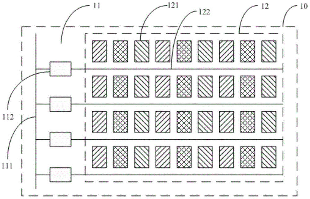
It can be seen from the figure that the gate driving circuit 112 and the driving signal line 111 in the prior art are located in the frame area 11, so in the actual manufacturing process, the width of the frame area 11 is relatively large, which is not conducive to the realization of a narrow frame
[0004] To sum up, the frame area of ​​the display panel in the prior art has a large width

Method used


Image

  • A display panel, a display device
  • A display panel, a display device
  • A display panel, a display device

Examples


Embodiment 1

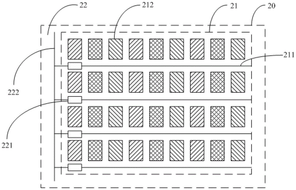
[0044] When the display panel in the specific embodiment of the present invention is an organic light emitting diode display panel, such as image 3 and Figure 4 As shown, the base substrate 20 is an OLED substrate, and the OLED substrate is divided into a display area 21 and a frame area 22 , the gate driving circuit 221 is located in the display area 21 , and the driving signal line 222 is located in the frame area 22 . Of course, in actual design, in order to further reduce the frame width of the display panel, both the gate driving circuit 221 and the driving signal line 222 may also be arranged in the display area 21 .

[0045] Preferably, the display area 21 of the organic light emitting diode substrate in the specific embodiment of the present invention includes a light-emitting area (not shown in the figure) and a non-light-emitting area (not shown in the figure), and the gate drive circuit 221 is arranged in the non-light-emitting area or, both the gate drive circui...

Embodiment 2

[0049] When the display panel in the specific embodiment of the present invention is an LCD display panel, reference can also be made to image 3 and Figure 4 As shown, the base substrate 20 is an array substrate, the array substrate is divided into a display area 21 and a frame area 22, the gate drive circuit 221 is located in the display area 21, and the driving signal line 222 is located in the frame area 22; of course, in actual design , both the gate driving circuit 221 and the driving signal line 222 may be arranged in the display region 21 , or the driving signal line 222 may be arranged in the display region 21 and the gate driving circuit 221 may be arranged in the frame region 22 . The specific design process of the gate driving circuit 221 and the driving signal line 222 when the display panel is an LCD display panel is similar to that when the display panel is an OLED display panel, and will not be repeated here.

[0050] The specific embodiment of the present in...


PUM


Abstract

The invention discloses a display panel and a display device, which are used for reducing the width of the frame area of ​​the display panel to realize narrow frame display. The display panel includes: a base substrate, the base substrate is divided into a display area and a frame area, the display area includes a plurality of gate lines arranged in an array, and the frame area surrounds the display area, wherein , the display panel also includes a gate driving circuit, and a driving signal line for controlling the operation of the gate driving circuit, each of the gate driving circuits is electrically connected to one of the gate lines, and the gate driving circuit Circuitry and / or the driving signal lines are located in the display area.

Description

technical field [0001] The present invention relates to the field of display technology, in particular to a display panel and a display device. Background technique [0002] The development direction of display technology is aimed at improving user experience, including improvement of display characteristics such as color gamut, high resolution (Pixel Per Inch, PPI), and high contrast. At present, with the popularization of civilian products such as mobile phones and televisions, higher requirements are gradually put forward for the frame design of the display panel. The advantage of the narrow bezel display is reflected in the ratio of the display area to the non-display area. The display panel with the narrow bezel display appears to have a larger display area, thereby improving the user experience. At the same time, narrow bezel products are also of great benefit to the application of splicing screens, which can reduce the width of the splicing joints of the splicing scr...

Claims


Application Information

Patent Timeline
Patent Type & Authority Patents(China)
IPC IPC(8): G09F9/30H01L27/32G02F1/133
CPCG02F1/13306G09F9/30H10K59/12
Inventor 李光刘利宾
Owner BOE TECH GRP CO LTD
Learn More