Method of depositing films

A thin film and surface deposition technology, applied in the direction of gaseous chemical plating, metal material coating process, coating, etc., can solve the problems of easy peeling off of carbon polymer particles and falling into the surface of semiconductor wafers, residues, etc.

Inactive Publication Date: 2015-03-25
SEMICON MFG INT (SHANGHAI) CORP
View PDF2 Cites 0 Cited by
  • Summary
  • Abstract
  • Description
  • Claims
  • Application Information

AI Technical Summary

Problems solved by technology

[0008] However, semiconductor wafers are usually placed in a crystal box, which is generally made of plastic, and the crystal box will age with time. The aged crystal box is easy to peel off carbon polymer particles and fall into the surface of the semiconductor wafer. Please refer to figure 2 , the surface of the semiconductor wafer 10 is covered with carbon polymer particles 20, when film deposition is performed, the film 30 will cover the carbon polymer particles 20, please refer to image 3 , some fine carbon polymer particles 20 may be dissociated by the plasma of the reaction gas, so the film 30 will have bubble defects (Bubble defect), and of course there will be larger carbon polymer particles 20 remaining under the film 30

Method used


Image

  • Method of depositing films
  • Method of depositing films
  • Method of depositing films

Examples


Embodiment Construction

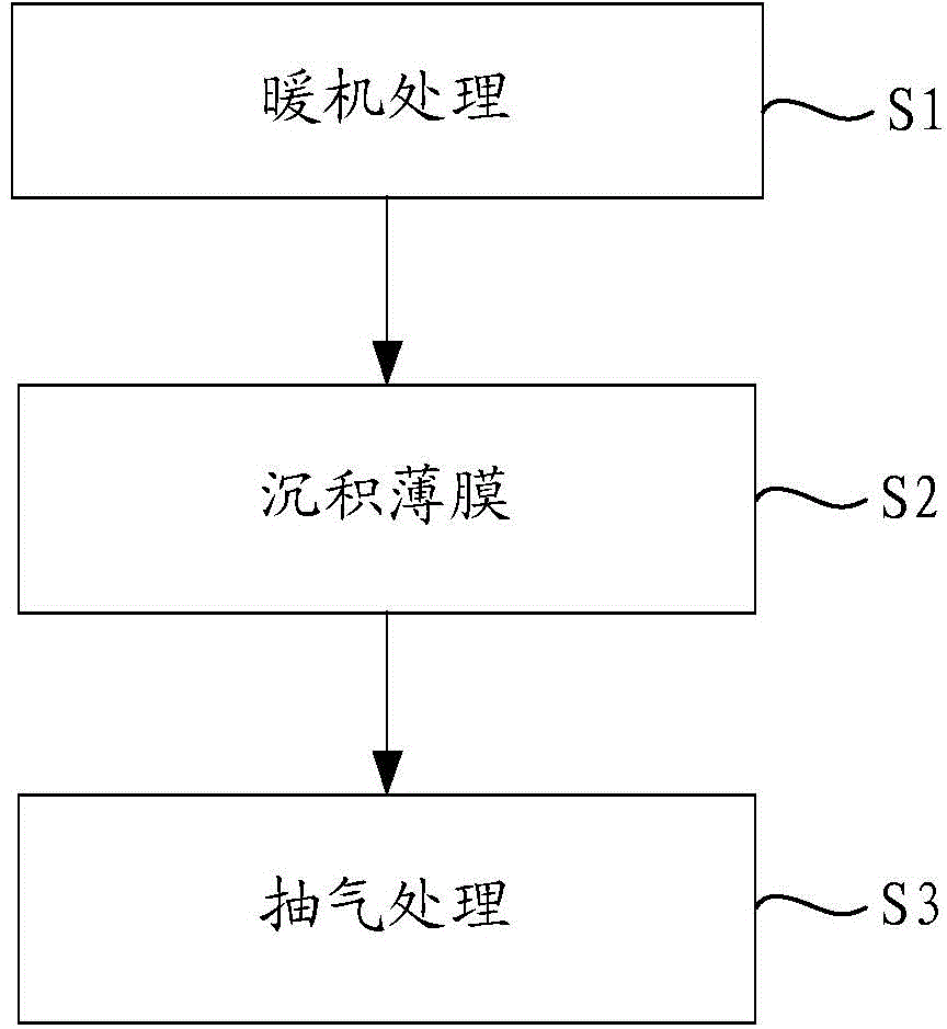
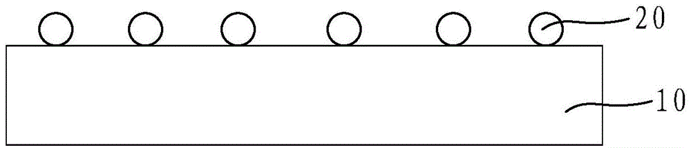
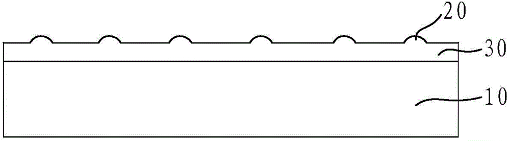
[0034] The method for depositing thin films of the present invention will be described in more detail below in conjunction with schematic diagrams, wherein a preferred embodiment of the present invention is represented, it should be understood that those skilled in the art can modify the present invention described here, and still realize the beneficial effects of the present invention . Therefore, the following description should be understood as the broad knowledge of those skilled in the art, but not as a limitation of the present invention.

[0035] In the interest of clarity, not all features of an actual implementation are described. In the following description, well-known functions and constructions are not described in detail since they would obscure the invention with unnecessary detail. It should be appreciated that in the development of any actual embodiment, numerous implementation details must be worked out to achieve the developer's specific goals, such as chan...


PUM


Abstract

The invention discloses a method of depositing films. The method comprises the following steps: performing film depositing on a semiconductor wafer, pre-treating the surface of the semiconductor wafer to remove carbon polymer particles remained on the surface of the semiconductor wafer, and then performing film deposition. The method of depositing films can be used for preventing formation of bubbly defects as the carbon polymer particles are covered below the films by virtue of the film deposition.

Description

technical field [0001] The invention relates to the field of semiconductor manufacturing, in particular to a method for depositing a thin film. Background technique [0002] In the semiconductor manufacturing process, a chemical vapor deposition (Chemical Vapor Deposit, CVD) process is usually used to deposit a thin film on the surface of a semiconductor wafer. Specifically, the reaction gas is dissociated into a plasma state and mixed in a reaction chamber, and a solid film is deposited on the surface of the semiconductor wafer. [0003] Please refer to figure 1 , figure 1 It is a flowchart of a method for depositing a thin film in an existing process, including steps: [0004] S1: warm-up processing; [0005] S2: deposition of thin film; [0006] S3: air extraction treatment. [0007] Among them, the warm-up treatment is to start the process of feeding the reaction gas and raising the temperature after the semiconductor wafer is placed in the reaction chamber, so tha...

Claims


Application Information

Patent Timeline
Patent Type & Authority Applications(China)
IPC IPC(8): C23C16/02
Inventor 李立春单伟中徐亮
Owner SEMICON MFG INT (SHANGHAI) CORP
Why Eureka
Try Eureka