
Dual-wavelength laser annealing device and method thereof

A dual-wavelength laser and annealing device technology, used in laser welding equipment, electrical components, circuits, etc., can solve the problems of short wavelength of 515nm laser, low crystal absorption energy, low activation rate, etc., and achieve excellent processing effect and annealing uniformity. High, improve the effect of activation rate

Active Publication Date: 2015-03-04
SUZHOU DELPHI LASER +1
View PDF5 Cites 10 Cited by
  • Summary
  • Abstract
  • Description
  • Claims
  • Application Information

AI Technical Summary

Problems solved by technology

The traditional process is to bake and anneal in an annealing furnace of quartz glass. Due to the low melting point of the aluminum base, the temperature of the annealing furnace can only be less than 450 degrees, resulting in low energy absorption by the crystal and a low activation rate after annealing. Due to the low cost, it is generally used Domestic low-end IGBT industry adopts
[0003] In order to improve the activation rate of implanted ions, laser annealing has been adopted by some manufacturers. Based on the pulsed green laser with variable pulse width, the activation rate of doped ions has been significantly improved. However, due to the short wavelength of the 515nm laser, the annealing The depth can only reach 1μm level, which cannot meet the deeper annealing process

Method used


Image

  • Dual-wavelength laser annealing device and method thereof

Examples


Embodiment Construction

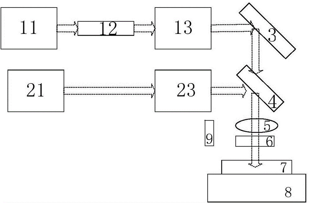
[0019] Such as figure 1 As shown, the dual-wavelength laser annealing device includes a green laser 11 and an infrared laser 21. On the output optical path of the green laser 11, a beam expander module 12, a green strip-shaped spot shaping module 13 and a green 45-degree reflector 3 are arranged in sequence. , the infrared strip spot shaping module 23 and the infrared 45-degree reflector 4 are arranged in sequence on the output light path of the infrared laser 21, the green light 45-degree reflector 3 and the infrared 45-degree reflector 4 can be a beam splitter, and the infrared laser light passes through the Reflecting mirror, combined with the reflected green laser beam, then output to the beam combining projection focusing mirror 5 at the rear end, the output optical path of the beam combining projection focusing mirror 5 is provided with an iris 6, and the output end of the iris 6 is facing Processing platform 8.

[0020] Wherein, the green laser 11 is a Q-switched pulse...


PUM

PropertyMeasurementUnit
lengthaaaaaaaaaa
widthaaaaaaaaaa
reflectanceaaaaaaaaaa

Abstract

The invention relates to a dual-wavelength laser annealing device and a method thereof. The dual-wavelength laser annealing device comprises a green laser device and an infrared laser device; an output optical path of the green laser device is sequentially provided with a beam expanding module, a green light bar-type spot reshaping module, and a green light 45-degree reflector; an output optical path of the infrared laser device is sequentially provided with an infrared bar-type spot reshaping module, and an infrared 45-degree reflector; output optical paths of the green light 45-degree reflector and the infrared 45-degree reflector are provided with a beam combining projection focus lens; an output optical path of the beam combining projection focus lens is provided with a variable diaphragm; and an output end of the variable diaphragm is directly opposite to a machining platform. Two laser beams are combined into one beam via the optical assembly; the combined laser beam is converted from a circular Gaussian distribution into a bar-type Gaussian distribution after being coordinated, adjusted and converted among optical elements; the laser is a bar-type light spot after the beam combination; the introduction of the infrared wavelength provides a deeper annealing depth for the light spot, makes the temperature rise at the moment that the laser contacts with the surface of material, thereby increasing the activation rate of implanted ions; and therefore the machining effect is better.

Description

technical field [0001] The invention relates to a silicon wafer back laser annealing device, in particular to a dual-wavelength laser annealing device and a method thereof. Background technique [0002] With the rapid development of the consumer electronics and home appliance industries, the high-voltage resistance of high-voltage integrated circuits is also gradually improving. High-voltage power integrated circuits enable devices to have both high transconductance and strong load driving capabilities of bipolar devices and high and low CMOS integration. advantage of power consumption. However, after the PSD (P-type heavily doped region) and NSD (N-type heavily doped region) process of this process, some crystals are not ordered and irregular, and an annealing process is required to change the order and improve activation rate. The traditional process is to bake and anneal in an annealing furnace of quartz glass. Due to the low melting point of the aluminum base, the temp...

Claims


Application Information

Patent Timeline
Patent Type & Authority Applications(China)
IPC IPC(8): H01L21/268B23K26/067
CPCB23K26/0643H01L21/268
Inventor 赵裕兴韩伟
Owner SUZHOU DELPHI LASER
Learn More