Image sensing module and manufacturing method thereof
A technology of image sensing and manufacturing method, applied in image communication, radiation control device, TV and other directions, can solve problems such as thickness reduction, and achieve the effect of reducing the assembly inclination angle
- Summary
- Abstract
- Description
- Claims
- Application Information
AI Technical Summary
Problems solved by technology
Method used
Image
Examples
no. 1 example 〕
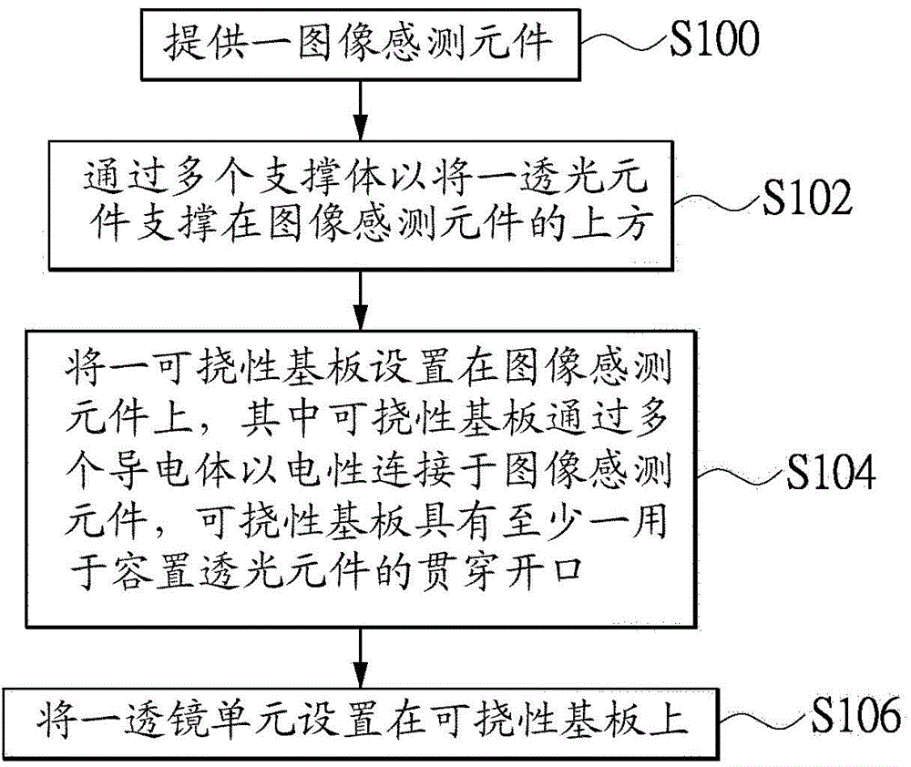
[0037] see Figure 1 to Figure 4 As shown, the first embodiment of the present invention provides a method for manufacturing an image sensing module M for reducing the overall thickness, which includes the following steps:
[0038] First, cooperate figure 1 and figure 2 As shown, an image sensing element 10 is provided, wherein the top of the image sensing element 10 has an image sensing region 100 ( S100 ). For example, the image sensing element 10 may be a Complementary Metal-Oxide-Semiconductor (CMOS) image sensing chip or any image sensor capable of image acquisition. However, the image sensing element 10 used in the present invention is not limited to the example mentioned in the first embodiment above.
[0039] Next, cooperate figure 1 and figure 2 As shown, a light-transmitting element 20 is supported above the image sensing element 10 by a plurality of supports 21, wherein the light-transmitting element 20 is located directly above the image sensing region 100 o...
no. 2 example
[0047] see Figure 5 As shown, the second embodiment of the present invention provides an image sensing module M for reducing the overall thickness, which includes: an image sensing unit 1 , a light transmission unit 2 , a substrate unit 3 and a lens unit 4 . The image sensing unit 1 includes an image sensing element 10 , wherein the top of the image sensing element 10 has an image sensing area 100 . The light-transmitting unit 2 includes a light-transmitting element 20 supported above the image sensing element 10 by a plurality of supports 21 , wherein the light-transmitting element 20 corresponds to the image sensing area 100 of the image sensing element 10 . The substrate unit 3 includes a flexible substrate 30 electrically connected to the image sensing device 10 . The lens unit 4 includes an opaque frame 40 disposed on the flexible substrate 30 and covering the transparent element 20 , and a lens assembly 41 connected to the opaque frame 40 and disposed above the transpa...
PUM
 Abstract
Description
Claims
Application Information
 - R&D Engineer
- R&D Manager
- IP Professional
- Industry Leading Data Capabilities
- Powerful AI technology
- Patent DNA Extraction
Browse by: Latest US Patents, China's latest patents, Technical Efficacy Thesaurus, Application Domain, Technology Topic, Popular Technical Reports.
© 2024 PatSnap. All rights reserved.Legal|Privacy policy|Modern Slavery Act Transparency Statement|Sitemap|About US| Contact US: help@patsnap.com


