


Quick Research
Generate reliable direction feasibility study reports for your R&D in just a few steps.

Technical Q&A
Discover and master advanced knowledge NOW. Basics, ideas, possibilities, all at once.

Find Solutions
As an expert in R&D theories, this can generate solutions to your technical problems instantly.

Evaluate Feasibility
Analyze your overall solution with one click, know your potential R&D risks in advance.

Monitor Landscape
Get weekly tech updates, stay abreast of the latest tech innovations and key insights.
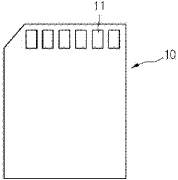
Semiconductor memory card, printed circuit board for memory card and method of fabricating the same
A technology for printed circuit boards and memory cards, applied in the field of memory cards, can solve problems such as reducing the yield of memory cards 10, and achieve the effects of preventing abnormal plating, reducing raw material costs, and reducing gold thickness
- Summary
- Abstract
- Description
- Claims
- Application Information
AI Technical Summary
Problems solved by technology
Method used
Image

Examples
Embodiment Construction
[0040] The embodiments will be described in detail with reference to the accompanying drawings so that those skilled in the art can easily use the embodiments. However, these embodiments may not be limited to the embodiments described below, but may have various modifications.
[0041] In the following description, when a predetermined component “includes” a predetermined component, the predetermined component does not exclude other components but may also include other components, and unless otherwise specified.
[0042] The thickness and size of each layer shown in the drawings may be exaggerated, omitted, or schematically drawn for convenience or clarity. Also, the size of elements does not utterly reflect an actual size. Throughout the drawings, the same reference numerals refer to the same elements.
[0043] In the description of embodiments, it will be understood that when a layer, film, region or panel is referred to as being "on" another layer, film, region or panel,...
PUM
| Property | Measurement | Unit |
|---|---|---|
| thickness | aaaaa | aaaaa |
| thickness | aaaaa | aaaaa |
| thickness | aaaaa | aaaaa |
Abstract
Description
Claims
Application Information
 - R&D Engineer
- R&D Manager
- IP Professional
- Industry Leading Data Capabilities
- Powerful AI technology
- Patent DNA Extraction
Browse by: Latest US Patents, China's latest patents, Technical Efficacy Thesaurus, Application Domain, Technology Topic, Popular Technical Reports.
© 2024 PatSnap. All rights reserved.Legal|Privacy policy|Modern Slavery Act Transparency Statement|Sitemap|About US| Contact US: help@patsnap.com