Defective pixel shielding method and system

A dead pixel and chip technology, applied in TV system components, TV, color TV components and other directions, can solve the problems of limited SRAM size, increased chip manufacturing cost, limited storage of dead pixel tables, etc. effect of size, reduced manufacturing size, reduced manufacturing cost

Active Publication Date: 2015-02-04
BEIJING VIMICRO ARTIFICIAL INTELLIGENCE CHIP TECH CO LTD
View PDF3 Cites 6 Cited by
  • Summary
  • Abstract
  • Description
  • Claims
  • Application Information

AI Technical Summary

Problems solved by technology

[0004] In view of this, the embodiment of the present invention provides a new method and system for covering dead pixels, which solves the problems in the prior art that due to the limited size of the SRAM in the chip, the storage of the bad pixel table is limited and the cost of chip manufacturing is increased.

Method used


Image

  • Defective pixel shielding method and system
  • Defective pixel shielding method and system
  • Defective pixel shielding method and system

Examples


Embodiment Construction

[0019] The technical solutions in the embodiments of the present invention will be clearly and completely described below in conjunction with the accompanying drawings in the embodiments of the present invention. Obviously, the described embodiments are only some, not all, embodiments of the present invention. Based on the embodiments of the present invention, all other embodiments obtained by persons of ordinary skill in the art without making creative efforts belong to the protection scope of the present invention.

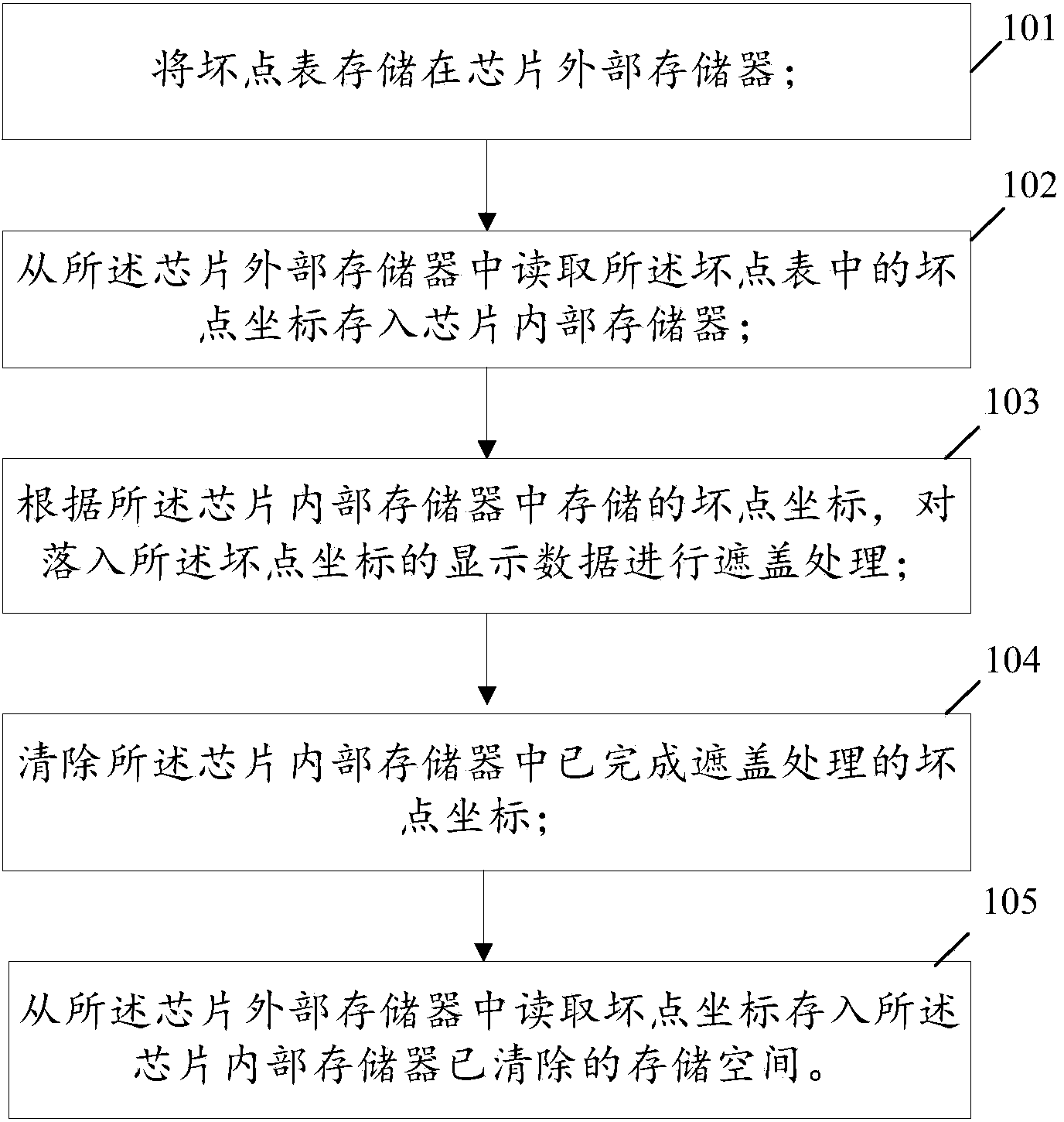
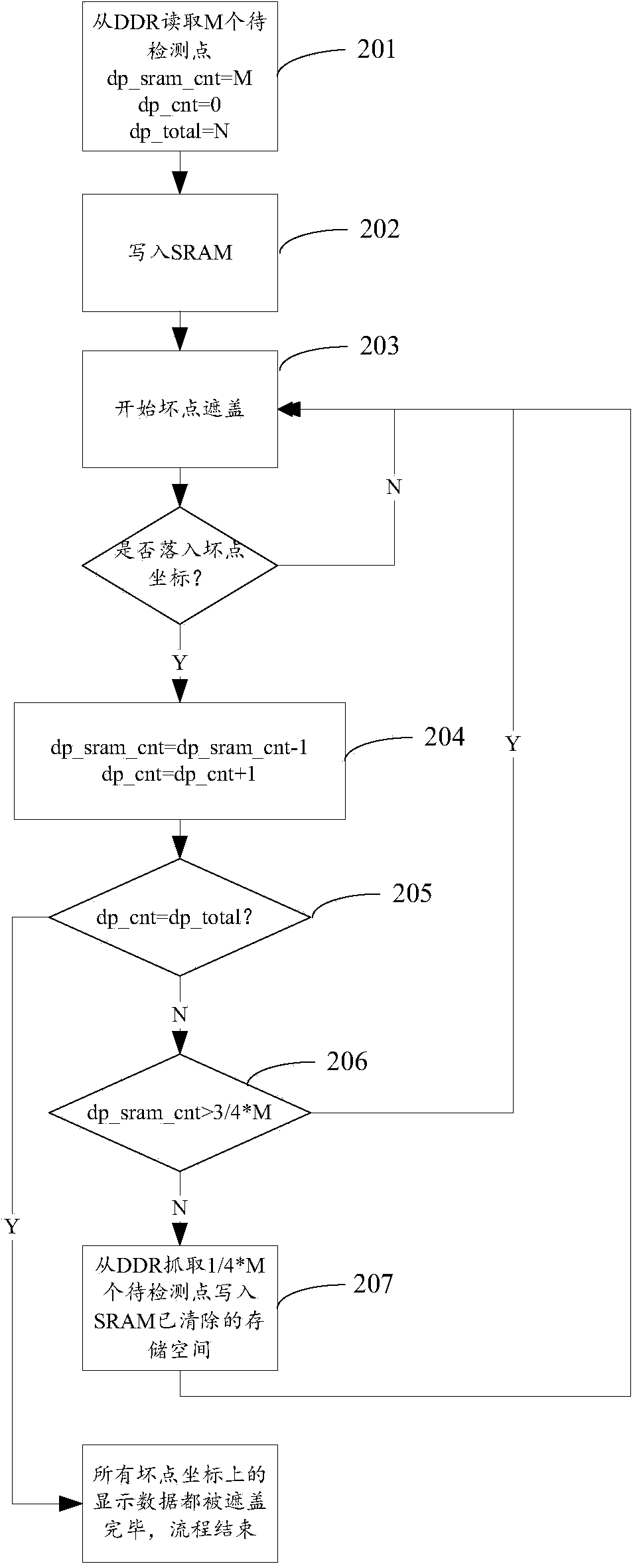
[0020] figure 1 Shown is a schematic flow chart of a bad pixel covering method provided by an embodiment of the present invention. Such as figure 1 As shown, the dead pixel covering method includes:

[0021] Step 101: Store the dead point table in the external memory of the chip. Wherein, the bad point table includes bad point coordinates of all bad points of the image sensor detected by a special program. In this way, in the subsequent covering step, only t...


PUM


Abstract

The embodiment of the invention provides defective pixel shielding method and system, and aims at solving the problem that the storage of a defective pixel table is limited and the manufacturing cost of a chip is increased due to the limitation on the size of an SRAM in the chip in the prior art. The defective pixel shielding method comprises the following steps: storing the defective pixel table into an external storage of the chip; reading the defective pixel coordinate in the defective pixel table from the outer storage of the chip into an inner storage of the chip; shielding and processing display data falling into the defective pixel coordinate according to the defective pixel coordinate stored in the inner storage of the chip; removing the shielded and processed defective pixel coordinates in the inner storage of the chip; continuously reading the defective pixel coordinate from the outer storage of the chip and then storing into the cleared storage space in the inner storage of the chip.

Description

technical field [0001] The invention relates to the field of digital image processing, in particular to a dead pixel covering method and system. technical background [0002] The dead point cover in the prior art is to first detect the dead point of the image sensor through a special program, and save the coordinates of the bad point in a bad point table; Processing is performed to cover the display data falling into the bad point coordinates with the cover algorithm. Among them, the dead point table is stored in the single-port SRAM (static memory) inside the chip. Existing SRAM generally can only store 1024 bad point coordinates, and the bit width of each bad point coordinate is 12-bit. [0003] However, with the continuous improvement of the resolution of the image sensor, the number of dead pixels of the image sensor and the bit width of the coordinates of the bad pixels are also continuously increased. Taking an image sensor with 4K resolution as an example, the bit ...

Claims


Application Information

Patent Timeline
Patent Type & Authority Applications(China)
IPC IPC(8): H04N5/21H04N17/00
Inventor 任立李国新吴大斌
Owner BEIJING VIMICRO ARTIFICIAL INTELLIGENCE CHIP TECH CO LTD
Why Eureka
Try Eureka