
Shift register unit, gate drive circuit, drive method thereof, and display panel

A shift register and gate connection technology, which is applied in the field of shift register unit, gate drive circuit and its driving method, and display panel, can solve the problem of increasing the complexity and difficulty of LTPS process, reducing TFT characteristics and yield, and improving product quality. cost and other issues, to achieve the effect of promoting promotion and application, reducing product cost, and improving functions

Active Publication Date: 2015-01-28
BOE TECH GRP CO LTD +1
View PDF5 Cites 71 Cited by
  • Summary
  • Abstract
  • Description
  • Claims
  • Application Information

AI Technical Summary

Problems solved by technology

However, in the traditional CMOS process, P-type and N-type thin film transistors (Thin Film Transistor, TFT) exist at the same time. In order to ensure the functionality and reliability of the circuit during the manufacturing process, it is necessary to make the N-type TFT and P-type TFT meet their respective performance. Requirements, thus increasing the complexity and difficulty of the LTPS process, reducing the TFT characteristics and yield, increasing the product cost, and limiting the CMOS LTPS GOA (Gate Driver on Array, array substrate row drive, or array substrate gate drive) application
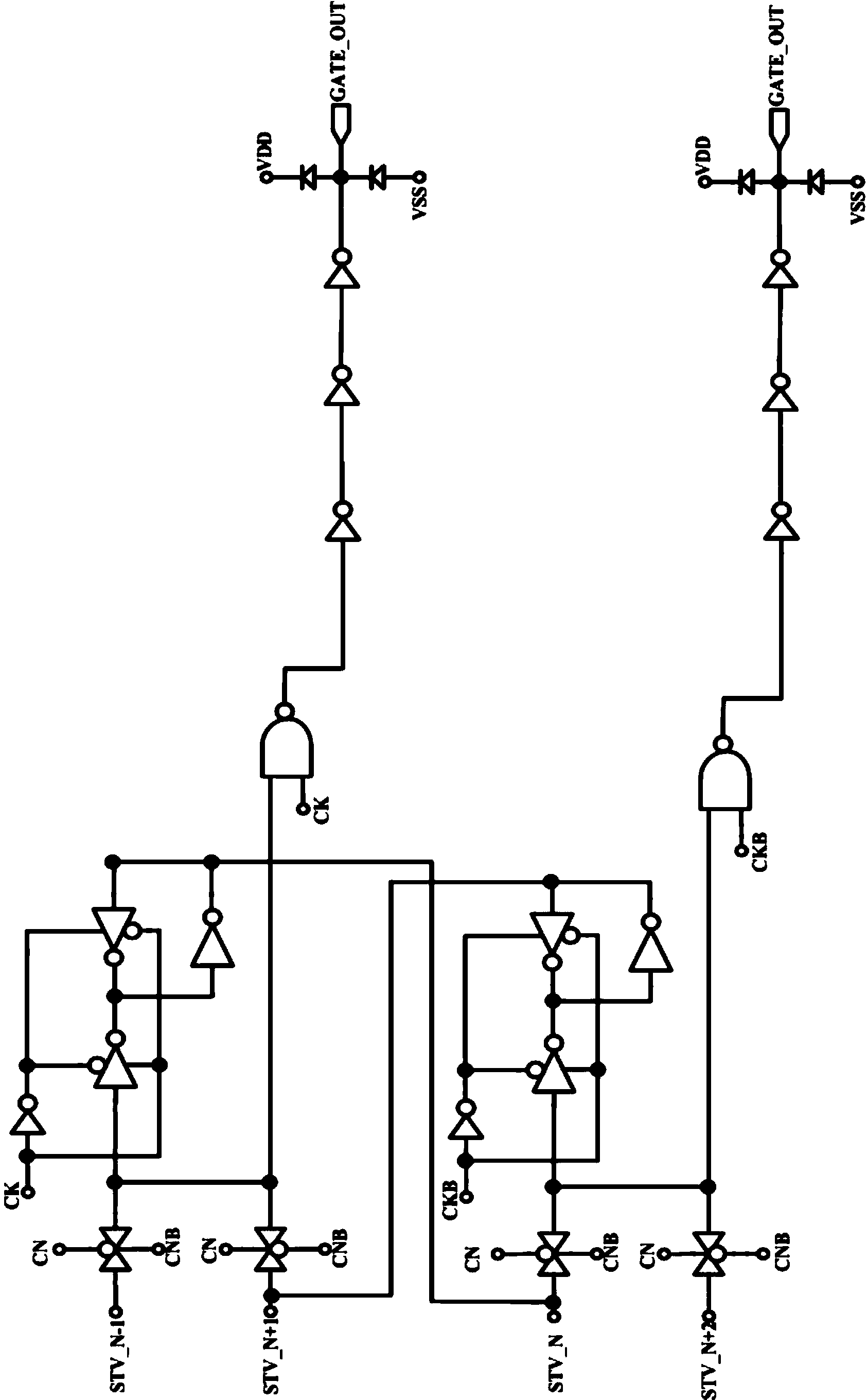
[0003] For example, if figure 1 A CMOS LTPS GOA circuit is shown, which is composed of latches, NAND gates, buffers and other parts. If these components are converted into thin film transistors, the circuit will include at least dozens of transistors. And the connection is extremely complex
At the same time, in order to ensure the functionality and reliability of the circuit, it is necessary to ensure the performance of N-type TFT and P-type TFT at the same time, which makes the process more difficult.

Method used


Image

  • Shift register unit, gate drive circuit, drive method thereof, and display panel
  • Shift register unit, gate drive circuit, drive method thereof, and display panel
  • Shift register unit, gate drive circuit, drive method thereof, and display panel

Examples


Embodiment Construction

[0049] In order to make the purpose, technical solutions and advantages of the embodiments of the present invention clearer, the technical solutions in the embodiments of the present invention will be clearly and completely described below in conjunction with the drawings in the embodiments of the present invention. Obviously, the described embodiments It is a part of embodiments of the present invention, but not all embodiments. Based on the embodiments of the present invention, all other embodiments obtained by persons of ordinary skill in the art without creative efforts fall within the protection scope of the present invention.

[0050] In the description of the present invention, it should be noted that the orientation or positional relationship indicated by the terms "upper", "lower", etc. is based on the orientation or positional relationship shown in the accompanying drawings, and is only for the convenience of describing the present invention and simplifying the descri...


PUM


Abstract

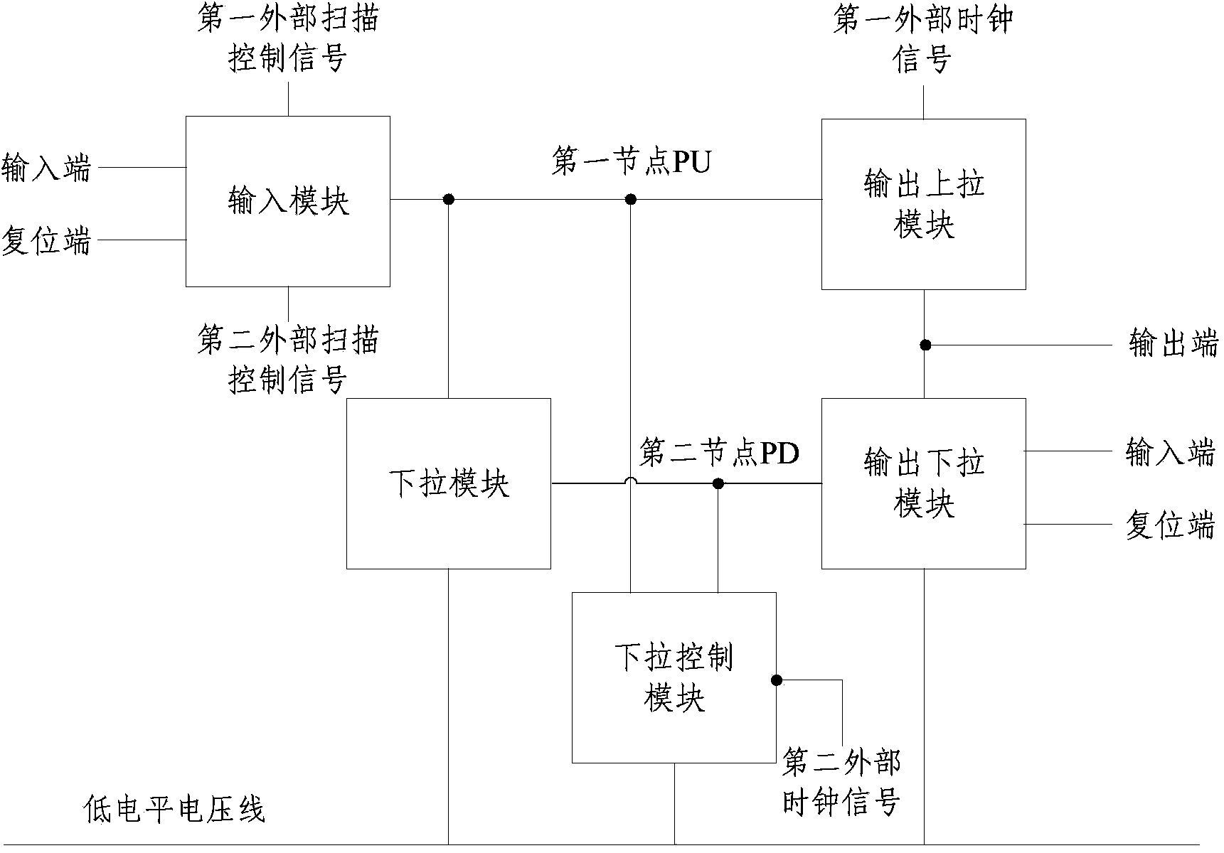
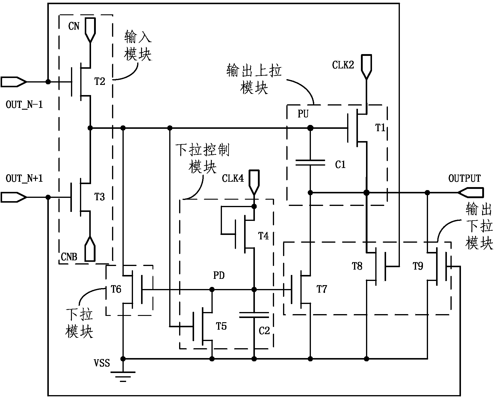
The invention provides a shift register unit, a gate drive circuit, a drive method of the gate drive circuit, and a display panel. The shift register unit comprises an input end, a reset end, an output end, an input module, a pull-down module, a pull-down control module, and an output pull-up module or an output pull-down module. Each module in the shift register unit only executes the specific voltage pull-up or pull-down function, and therefore can be formed by a single N-type TFT or a single P-type TFT. Compared with a CMOS, an LTPS and a GOA in the prior art, the shift register unit and the gate drive circuit have the advantages of being simple in structure, complete in function, and high in quality and reliability, the process is simple and easy to implement, the product cost can be reduced easily, and the application and the popularization of the CMOS, the LTPS and the GOA are promoted.

Description

technical field [0001] The invention relates to the field of display technology, in particular to a shift register unit, a gate drive circuit and a drive method thereof, and a display panel. Background technique [0002] Currently, Complementary Metal Oxide Semiconductor (CMOS) low temperature polysilicon (LTPS) technology is usually applied in LTPS liquid crystal display (Liquid Crystal Display, LCD). The gate driving circuit integrated according to the CMOS process has a simple structure, and has the advantages of high reliability and low power consumption. However, in the traditional CMOS process, P-type and N-type thin film transistors (Thin Film Transistor, TFT) exist at the same time. In order to ensure the functionality and reliability of the circuit during the manufacturing process, it is necessary to make the N-type TFT and P-type TFT meet their respective performance. Requirements, thus increasing the complexity and difficulty of the LTPS process, reducing the TFT...

Claims


Application Information

Patent Timeline
Patent Type & Authority Applications(China)
IPC IPC(8): G09G3/36G11C19/28
CPCG09G2310/0283G11C19/287G09G3/3677G09G2310/0286G09G2310/08G11C19/28G09G3/3688G09G2300/0809
Inventor 吴博邓银祁小敬谭文
Owner BOE TECH GRP CO LTD
Learn More