An electric anti-peeping film and its preparation method
A technology of anti-spy film and electrochromic layer, which is applied in the direction of chemical instruments and methods, coatings, layered products, etc., can solve the problems of poor light transmittance of anti-spy film and unadjustable anti-spy function, and achieve light transmission high rate effect
- Summary
- Abstract
- Description
- Claims
- Application Information
AI Technical Summary
Problems solved by technology
Method used
Image
Examples
Embodiment 1
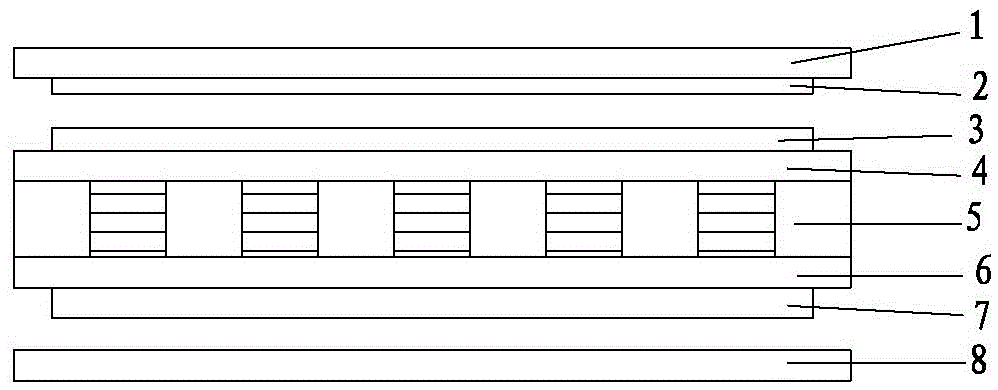
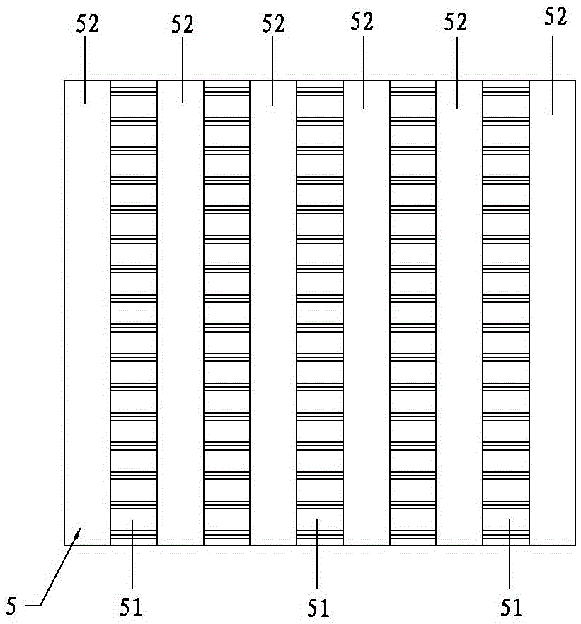
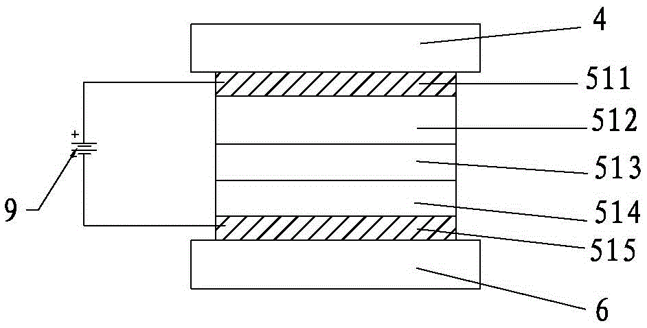
[0066] An electric anti-peeping film in this embodiment includes a protective film layer 1, a first adhesive layer 2, a hardened layer 3, a first main film layer 4, a louver layer 5, and a second main film arranged in sequence from top to bottom. Layer 6, the second adhesive layer 7 and the peeling layer 8, and electrodes 9 are connected between the upper surface and the lower surface of the louver layer 5. The louver layer 5 of the present embodiment includes a plurality of louver units 51, and the louver unit 51 is filled with a photocurable resin unit 52, and each louver unit 51 is composed of a first TC transparent conductive layer 511, an EL ion conductor layer 512, an EC electrochromic Layer 513, CE ion storage layer 514 and second TC transparent conductive layer 515 are stacked in sequence. Specifically, the first TC transparent conductive layer 511 and the second TC transparent conductive layer 515 are respectively connected to the electrodes 9 through electrode wires....
Embodiment 2
[0080] The hardened layer of the present embodiment and the photocurable resin unit are all composed of the following photocurable resin raw materials in weight percentage: 61% epoxy acrylate, 7% polyurethane acrylate, 8% methyl methacrylate, 8% butyl acrylate %, hydroxyethyl acrylate 6%, benzoin ethyl ether 5%, benzophenone 2%, triethanolamine 1%, leveling agent 1%, photosensitizer 1%. The curing energy of photocurable resin raw material is 500mj / cm 2 , The curing time is 14s.
[0081] The thickness of the first TC transparent conductive layer and the second TC transparent conductive layer is 75nm, the surface resistance is 600Ω, the thickness of the EL ion conductor layer is 10μm, the thickness of the EC electrochromic layer is 1μm, and the electrochromic material is IrO 3 , the thickness of the CE ion storage layer is 10 μm.
[0082] The thickness of the protective film layer is 50 μm, the thickness of the first adhesive layer is 10 μm, the thickness of the hardened layer...
Embodiment 3
[0086] The hardened layer of the present embodiment and the photocurable resin unit are all made up of the following photocurable resin raw materials in weight percentage: epoxy acrylate 62%, polyurethane acrylate 6.5%, methyl methacrylate 7.5%, butyl acrylate 8% %, 7% hydroxyethyl acrylate, 4% benzoin ethyl ether, 2% benzophenone, 0.5% triethanolamine, 0.5% leveling agent, and 2% photosensitizer. The curing energy of photocurable resin raw material is 600mj / cm 2 , The curing time is 13s.
[0087] The thickness of the first TC transparent conductive layer and the second TC transparent conductive layer is 100nm, the surface resistance is 700Ω, the thickness of the EL ion conductor layer is 30μm, the thickness of the EC electrochromic layer is 5μm, and the electrochromic material is IrOx, IrOx It is a mixture of IrO2 and IrO3 blended at a mass ratio of 1:1, and the thickness of the CE ion storage layer is 30 μm.
[0088] The thickness of the protective film layer is 75 μm, the...
PUM
| Property | Measurement | Unit |
|---|---|---|
| thickness | aaaaa | aaaaa |
| thickness | aaaaa | aaaaa |
| thickness | aaaaa | aaaaa |
Abstract
Description
Claims
Application Information
 - R&D Engineer
- R&D Manager
- IP Professional
- Industry Leading Data Capabilities
- Powerful AI technology
- Patent DNA Extraction
Browse by: Latest US Patents, China's latest patents, Technical Efficacy Thesaurus, Application Domain, Technology Topic, Popular Technical Reports.
© 2024 PatSnap. All rights reserved.Legal|Privacy policy|Modern Slavery Act Transparency Statement|Sitemap|About US| Contact US: help@patsnap.com


