
Infrared imaging detector carbon nanotube based on quantum dots and preparation method for the same

A technology of carbon nanotubes and infrared imaging, which is applied in semiconductor devices, final product manufacturing, sustainable manufacturing/processing, etc., can solve problems such as the difficulty of obtaining parallel arrays of carbon nanotubes and the failure to realize high-performance detection devices, and achieve the goal of reducing dark The effect of current level, improved detection rate, and simplified process

Inactive Publication Date: 2014-11-26
PEKING UNIV
View PDF7 Cites 6 Cited by
  • Summary
  • Abstract
  • Description
  • Claims
  • Application Information

AI Technical Summary

Problems solved by technology

Although the light absorption coefficient of carbon nanotubes is very large, it is difficult to obtain parallel arrays of high-purity and high-density semiconducting carbon nanotubes, so high-performance detectors based on a single material of carbon nanotubes have not been realized.

Method used

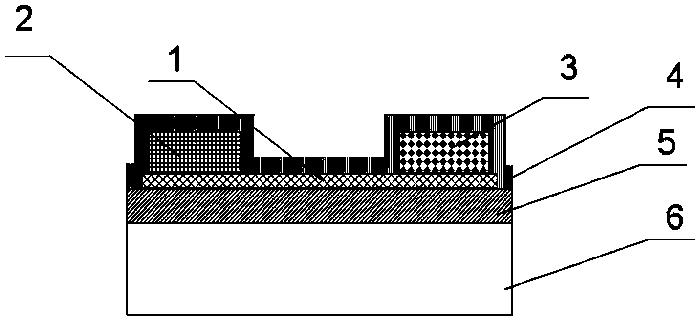
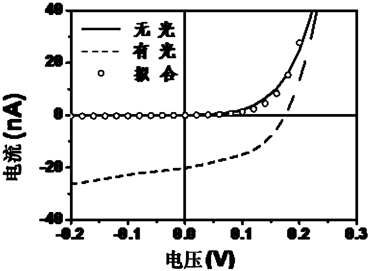
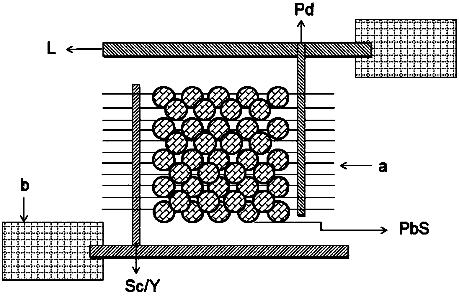

Image

  • Infrared imaging detector carbon nanotube based on quantum dots and preparation method for the same
  • Infrared imaging detector carbon nanotube based on quantum dots and preparation method for the same
  • Infrared imaging detector carbon nanotube based on quantum dots and preparation method for the same

Examples


Embodiment Construction

[0052] The present invention will be further described below through specific embodiments and accompanying drawings.

[0053] The infrared imaging detector of the present invention can use several one-dimensional semiconducting carbon nanotubes or several semiconducting carbon nanotube thin film strips, which are similar in the device preparation process. Combining the near-infrared PbS quantum dot material to form a quantum dot-carbon nanotube composite material infrared imaging detector. image 3 It is the basic form of infrared imaging detector using quantum dot-semiconducting carbon nanotube thin film strips. The width of the two asymmetric electrodes on the semiconducting carbon nanotube thin film strip is 1 micron, and the distance between the two asymmetric electrodes is 10 microns. The specific process steps are as follows:

[0054] 1) Obtain the Si / SiO 2 Intrinsically high-density semiconducting carbon nanotube thin film strips a on substrates in Si / SiO using evapora...


PUM


Abstract

The invention discloses an infrared imaging detector carbon nanotube based on quantum dots and a preparation method for the same. The infrared imaging detector comprises a substrate, a plurality of one dimensional semiconductor carbon nanotubes or semiconductor carbon nanotube thin film strips which are positioned on the substrate, an asymmetric contact electrode for forming contact of electrons and electron hole ohmics and a plurality of Pbs quantum dots, wherein the asymmetric contact electrode comprises a plurality of first electrodes and a plurality of second electrodes. A plurality of one dimensional semiconductor carbon nanotubes or a plurality of semiconductor carbon nanotube thin film strips are arranged on the substrate by the evaporation drive self-assembling method; a first electrode, a second electrode and pattern shapes of metal connection lines are formed on the substrate; the metal layer of the electrode is evaporated; and the quantum dots are deposited on the carbon nanotube thin film in the middle of the conducting channel. The invention can obtain high detection efficiency, can solve the unstable problem of the short chain converted from the quantum dot, and can provide convenience to production.

Description

technical field [0001] The invention relates to an infrared light detector, in particular to an infrared imaging detector prepared based on PbS quantum dots and semiconducting carbon nanotubes, and a preparation method thereof. Background technique [0002] Infrared light detection is a very important direction in the field of light detection, and has been widely used in scientific fields as well as industrial and military applications, including monitoring, manufacturing process control, optical communication, biological and military night detection. Infrared light detectors based on various materials are currently the research hotspots of scientists from all over the world. Infrared photodetectors based on traditional semiconductor materials can achieve high quantum efficiency and good extreme detection performance at low temperatures, and can achieve high detection and fast response speed. However, due to the high technical difficulty and complex process , the price is h...

Claims


Application Information

Patent Timeline
Patent Type & Authority Applications(China)
IPC IPC(8): H01L31/0224H01L31/18H01L31/101
CPCH01L31/0224H01L31/035218H01L31/101H01L31/1828Y02P70/50
Inventor 刘旸王胜魏楠彭练矛
Owner PEKING UNIV
Learn More