Pixel cell structure, array structure and display device

A pixel unit and sub-pixel unit technology, applied in electrical components, semiconductor devices, circuits, etc., can solve the problems of low luminous efficiency of OLED display devices and high power consumption of OLED display devices

Active Publication Date: 2014-11-19
WUHAN TIANMA MICRO ELECTRONICS CO LTD +1
View PDF3 Cites 8 Cited by
  • Summary
  • Abstract
  • Description
  • Claims
  • Application Information

AI Technical Summary

Problems solved by technology

[0006] After research, the inventor found that in the prior art, there are problems of high power

Method used


Image

  • Pixel cell structure, array structure and display device
  • Pixel cell structure, array structure and display device
  • Pixel cell structure, array structure and display device

Examples


Embodiment Construction

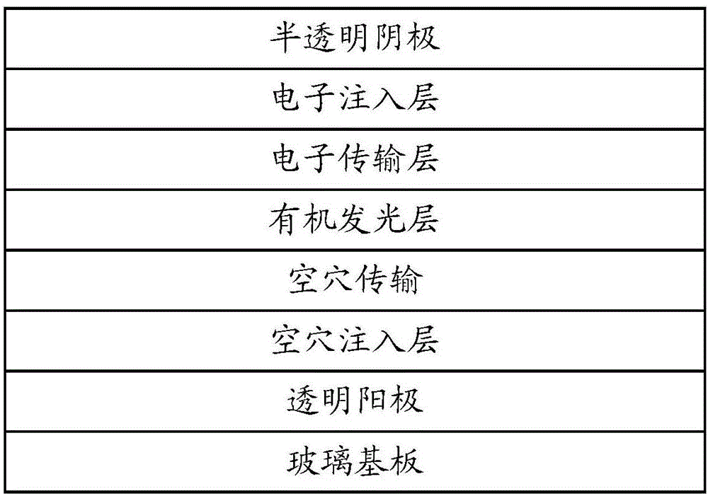
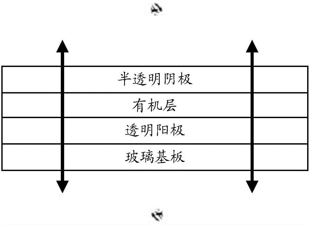
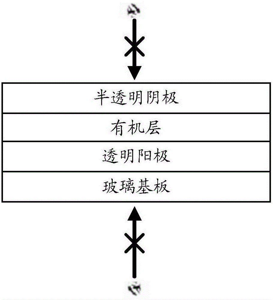
[0030] In order to solve the problems of high power consumption of the OLED display device and low luminous efficiency of one side of the OLED display device in the prior art. In an embodiment of the present invention, a pixel unit structure is provided, and the pixel unit structure includes a sub-pixel unit group and a first sub-pixel unit in another sub-pixel unit group adjacent to the sub-pixel unit group; wherein, the sub-pixel The unit group includes a second sub-pixel unit and a third sub-pixel unit, the first sub-pixel unit, the second sub-pixel unit and the third sub-pixel unit all include a light-emitting area, the first sub-pixel unit, the second sub-pixel unit or the third sub-pixel unit Any sub-pixel unit in the three sub-pixel units includes a light-transmitting area; and, the light-emitting areas in the first sub-pixel unit, the second sub-pixel unit, and the third sub-pixel unit all include the first substrate and the second sub-pixel unit arranged in sequence. ...


PUM


Abstract

The invention provides a pixel cell structure, an array structure and a display device. The pixel cell structure includes a sub pixel cell group and a first sub pixel cell adjacent to the sub pixel cell group, wherein the sub pixel cell group includes a second sub pixel cell and a third sub pixel cell, light emitting areas are included in the first sub pixel cell, the second sub pixel cell and the third sub pixel cell, and a light transmitting area is included in any of the sub pixel cells. The light emitting area of each of the first sub pixel cell, the second sub pixel cell and the third sub pixel cell adopts a top emission structure which adopts an opaque anode and a semi-transparent cathode to achieve single side top light emission, thereby reducing the power consumption of the display device. The adjacent sub pixel cell group and first sub pixel cell form a pixel cell structure, the light transmitting area is added into any of the sub pixel cells, and the light transmittance of a display panel is effectively improved through the light transmitting area.

Description

technical field [0001] The invention relates to the field of transparent display, in particular to a pixel unit structure, an array structure and a display device. Background technique [0002] Compared with the currently widely used liquid crystal and plasma display devices, OLED (Organic Light-Emitting Diode; Organic Light-Emitting Diode) display devices are self-illuminating, rich in color, fast in response, wide in viewing angle, light in weight, thin in thickness, and power-consuming. The advantages of less, flexible display and other advantages have attracted much attention. [0003] Generally, an OLED display device is composed of a glass substrate, an ITO (indium tin oxide) anode (Anode), an organic layer (including an organic light emitting layer (Emitting Material Layer)) and a translucent cathode (Cathode). Wherein, when a voltage is injected into the anode, the holes (Hole) of the anode and the electrons (Electron) of the cathode combine in the organic light-emi...

Claims


Application Information

Patent Timeline
IPC IPC(8): H01L27/32H01L51/52
CPCH10K59/353H10K59/121
Inventor 吕伯彦罗丽媛钱栋
Owner WUHAN TIANMA MICRO ELECTRONICS CO LTD
Why Eureka
Try Eureka