Integrated parallel optical assembly and optical transceiver module
A technology of optical components and optical paths, which is applied in the field of optical communication, can solve the problems of increasing the electrical parasitic effect of optical components, limiting the transmission rate of the system, and high manufacturing costs, and achieves the effects of reducing electrical parasitic effects, simple process, and low cost
- Summary
- Abstract
- Description
- Claims
- Application Information
AI Technical Summary
Problems solved by technology
Method used
Image
Examples
Embodiment 1
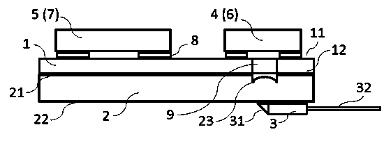
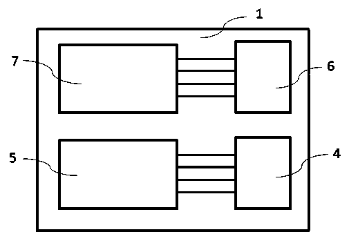
[0027] Such as figure 1 and figure 2 As shown, the integrated parallel optical component of this embodiment includes a circuit board 1 , a transparent substrate 2 , a 90-degree optical path bending connector 3 , a laser array 4 , a driver 5 , a photodetector array 6 and a transconductance amplifier 7 . Both the laser array 4 and the photodetector array 6 are four parallel arrays. The laser in this embodiment is a vertical cavity surface emitting laser (VCSEL).
[0028] The first side 11 of the circuit board 1 is arranged with an electrode array 8, and the VCSEL array 4, driver 5, photodetector array 6 and transconductance amplifier 7 are mounted on the first side of the circuit board 1 in a flip-chip bonding manner. side 11 and is electrically connected to the electrode array 8 . The arrangement of the VCSEL array 4, driver 5, photodetector array 6 and transconductance amplifier 7 on the circuit board 1 is as follows: figure 2 shown. In this embodiment, a lens 23 is pro...
Embodiment 2
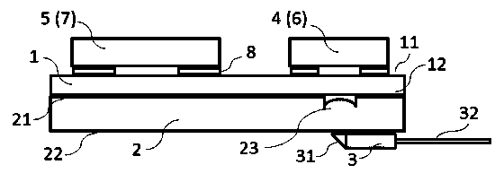
[0032] The difference between this embodiment and the first embodiment is that the light transmission device provided on the circuit board 1 is realized by using a transparent substrate.
[0033] Such as figure 2 and image 3 As shown, the integrated parallel optical component of this embodiment includes a circuit board 1 , a transparent substrate 2 , a 90-degree optical path bending connector 3 , a laser array 4 , a driver 5 , a photodetector array 6 and a transconductance amplifier 7 . Both the laser array 4 and the photodetector array 6 are four parallel arrays. The laser in this embodiment is a vertical cavity surface emitting laser (VCSEL).
[0034]The first side 11 of the circuit board 1 is arranged with an electrode array 8, and the VCSEL array 4, driver 5, photodetector array 6 and transconductance amplifier 7 are mounted on the first side of the circuit board 1 in a flip-chip bonding manner. side 11 and is electrically connected to the electrode array 8 . The arr...
Embodiment 3
[0039] This embodiment is a parallel optical transceiver module using any one of the integrated parallel optical components described in Embodiment 1 or Embodiment 2. Preferably, the integrated parallel optical component of Embodiment 2 is used.
[0040] The integrated parallel optical transceiver module of this embodiment includes a circuit substrate, a housing, a parallel optical fiber pluggable interface and an integrated parallel optical component. Both the circuit substrate and the integrated parallel optical components are packaged in the housing. The circuit substrate is electrically connected to the integrated parallel optical module, and the electrical interface of the parallel optical module adopts gold finger electrodes. Both the VCSEL array 4 and the photodetector array 6 of the present embodiment are 4-way, and the parallel optical fiber pluggable interface is 12 channels, wherein 4 channels are coupled with 4 VCSEL coupling pairs of the VCSEL array 4 of the integ...
PUM
 Abstract
Description
Claims
Application Information
 - Generate Ideas
- Intellectual Property
- Life Sciences
- Materials
- Tech Scout
- Unparalleled Data Quality
- Higher Quality Content
- 60% Fewer Hallucinations
Browse by: Latest US Patents, China's latest patents, Technical Efficacy Thesaurus, Application Domain, Technology Topic, Popular Technical Reports.
© 2025 PatSnap. All rights reserved.Legal|Privacy policy|Modern Slavery Act Transparency Statement|Sitemap|About US| Contact US: help@patsnap.com


