
Detection method and device for direct current transmission design

A technology of direct current and detection methods, applied in measuring devices, computer-aided design, calculations, etc., can solve problems such as difficulty in finding causes, consuming material resources, and consuming manpower, and achieve efficient and reliable detection effects

Inactive Publication Date: 2014-09-24
HONG FU JIN PRECISION IND (SHENZHEN) CO LTD +1
View PDF0 Cites 1 Cited by
  • Summary
  • Abstract
  • Description
  • Claims
  • Application Information

AI Technical Summary

Problems solved by technology

After this simple design method is made into a product, once there is a problem with the current, it is often difficult to find the cause, and even if the cause is found, redesigning the PCB will consume manpower and material resources.

Method used


Image

  • Detection method and device for direct current transmission design
  • Detection method and device for direct current transmission design

Examples


Embodiment Construction

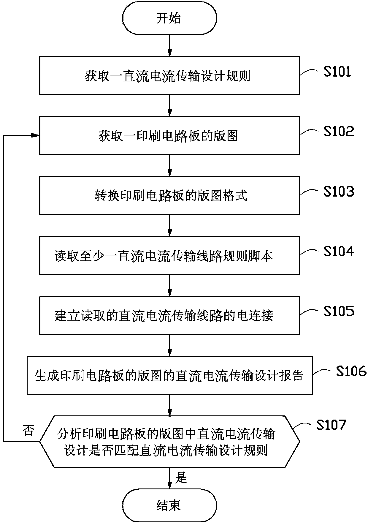
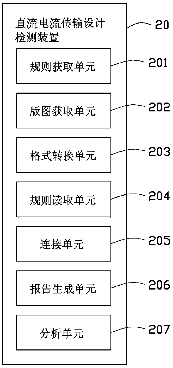
[0033] see figure 1 , the figure schematically shows a flow chart of a method for detecting a DC current transmission design of a printed circuit board according to an embodiment of the present invention, and the method includes the following steps:

[0034] Step S101, obtaining a DC current transmission design rule. The DC current transmission design rules of the printed circuit board are used to provide several DC current transmission line design rules.

[0035] Step S102, acquiring a layout of a printed circuit board. The layout of the printed circuit board can be a digital layout directly drawn by a layout drawing tool, such as a layout file with the suffix .brd generated by Cadence allegro layout design software, or it can be a photograph or scan of the printed circuit board via an image acquisition tool Generated digital layout.

[0036] Step S103, converting the layout format of the printed circuit board. The format of the layout of the printed circuit board can be ...


PUM


Abstract

The invention relates to a detection method for direct current transmission design. The method comprises the following steps: acquiring a direct current transmission design rule, wherein the rule comprises at least a direct current transmission route design rule; acquiring a printed circuit board layout; reading a script of the direct current transmission route design rule corresponding to the printed circuit board layout; examining whether a specified direct current transmission route in the printed circuit board layout is matched with the direct current transmission design rule or not, and generating a direct current transmission route report of the printed circuit board; analyzing the direct current transmission route report in the printed circuit board layout; when the direct current transmission route report is mismatched with the direct current transmission design rule, analyzing the copper foil width of the specific direct current transmission route in the printed circuit board layout according to report data; when the direct current transmission route report is matched with the direct current transmission design rule, ending the detection. The invention further discloses a detection device for the direct current transmission design of the printed circuit. According to the technical scheme of the invention, the direct current transmission design of the printed circuit board can be efficiently and reliably detected.

Description

technical field [0001] The invention relates to the field of printed circuit boards, in particular to a method and device for detecting the direct current transmission design of a printed circuit board. Background technique [0002] The normal operation of integrated chips on electronic products first needs to receive stable and reliable DC current from the current pin (power pin) of the integrated chip (IC), such as 5V, 3V, 1.8V, etc., which are at the receiving end (pin) The voltage fluctuation of the chip generally cannot exceed a range, such as + / -5%, if the voltage received here exceeds this range, the chip will not work properly. Before the power pin, the DC current needs to be transmitted on the PCB, that is, through the copper foil on the Printed Circuit Board (PCB) used to transmit the current, and sometimes includes small resistance and small inductance between the copper foils For low-resistance passive parts, not only small resistance and small inductance will c...

Claims


Application Information

Patent Timeline
Patent Type & Authority Applications(China)
IPC IPC(8): G06F17/50
CPCG06F17/5081G01R31/3185G06F30/398
Inventor 林有旭吴政达欧光峰
Owner HONG FU JIN PRECISION IND (SHENZHEN) CO LTD
Learn More