TFT array substrate structure

An array substrate structure and black matrix technology, which is applied in optics, instruments, electrical components, etc., can solve problems such as different brightness, dark brightness, and changes in electric field, so as to achieve the effect of improving quality, improving electrical characteristics, and avoiding dark lines

Inactive Publication Date: 2014-08-27
TCL CHINA STAR OPTOELECTRONICS TECH CO LTD
View PDF5 Cites 16 Cited by
  • Summary
  • Abstract
  • Description
  • Claims
  • Application Information

AI Technical Summary

Problems solved by technology

During the bending process, since the TFT array substrate and the color filter substrate are based on the center of the panel, relative displacements will gradually occur along the left and right sides in the horizontal direction, causing the relative displacement of the pixel electrode trunk of the TFT array substrate, which in turn causes the electric field to change, resulting in Curved liquid crystal display device produces dark lines corresponding to the position near the trunk of the pixel electrode
The more serious problem is that the relative displacement area caused by the bending of the liquid crystal panel is based on the center of the panel, and gradually expands to the left and right sides, causing the areas with large displacement on the left and right sides to have different brightness from the area without relative displacement in the middle, that is, the displacement is relatively large. The brightness of large areas is dim, making the entire panel poorly displayed

Method used


Image

  • TFT array substrate structure
  • TFT array substrate structure
  • TFT array substrate structure

Examples


Embodiment Construction

[0022] In order to further illustrate the technical means adopted by the present invention and its effects, the following describes in detail in conjunction with preferred embodiments of the present invention and accompanying drawings.

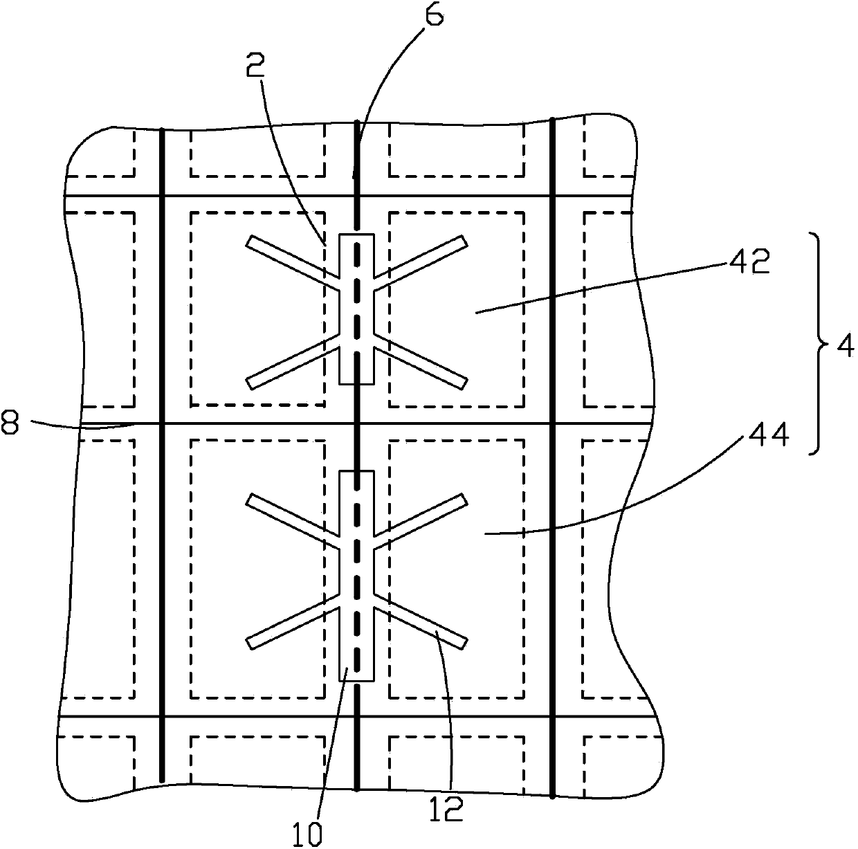
[0023] see image 3 , the present invention provides a TFT array substrate structure, including: several sub-pixels 4 arranged corresponding to the black matrix 2 on the color filter substrate, and each sub-pixel 4 includes a main area 42 and a sub-area 44 arranged corresponding to the black matrix 2 A data line 6 is provided between the sub-pixels, a gate scanning line 8 is provided between the main area 42 and the sub-area 44, and a pixel electrode trunk 10 is provided between two adjacent sub-pixels 4. Pixel electrode branches 12 are respectively disposed on the main area 42 and the sub area 44 of the pixel 4 , and the pixel electrode branches 12 are respectively electrically connected to the pixel electrode trunk 10 .

[0024] The pixel e...


PUM


Abstract

The invention provides a TFT array substrate structure. The TFT array substrate structure comprises a plurality of sub-pixels (4) arranged corresponding to black arrays (2). Each sub-pixel (4) comprises primary areas (42) and secondary areas (44) arranged corresponding to the corresponding black arrays (2). A data line (6) is arranged between every two adjacent sub-pixels. A grid scanning line (8) is arranged between each primary area (42) and the corresponding secondary area (44). A pixel electrode trunk (10) is arranged between every two adjacent sub-pixels (4). Pixel electrode branches (12) are arranged on the primary areas (42) and the secondary areas (44) of every two adjacent sub-pixels (4) respectively. The pixel electrode branches (12) are electrically connected with the pixel electrode trunks (10) respectively. When relative displacement happens to the TFT array substrate structure in the bending process of a liquid crystal display panel, the pixel electrode branches (10) are still in the areas covered by the black arrays, the influences on the electric field are extremely small, the electrical properties can be effectively increased, dark fringes are avoided, and therefore quality of the liquid crystal display panel is improved.

Description

technical field [0001] The present invention relates to the field of liquid crystal display, in particular to a TFT (Thin Film Transistor, thin film transistor) array substrate structure. Background technique [0002] Liquid crystal display (Liquid Crystal Display, LCD) has many advantages such as thin body, power saving, and no radiation, and has been widely used, such as mobile phones, personal digital assistants (PDA), digital cameras, computer screens or notebook computer screens Wait. [0003] Generally, a liquid crystal display device includes a housing, a liquid crystal display panel disposed in the housing, and a backlight module disposed in the housing. Such as figure 1 As shown, the existing liquid crystal display panel includes a TFT array substrate 100, a color filter substrate (Color Filter, CF) 300 located above the TFT array substrate 100 and attached to it, Between the liquid crystal layer (Liquid Crystal Layer) 500 and the sealant frame 700, its working p...

Claims


Application Information

Patent Timeline
Patent Type & Authority Applications(China)
IPC IPC(8): G02F1/1343G02F1/1362
CPCG02F1/134336G02F1/134345G02F1/133512G02F1/133514G02F1/13439G02F1/136286G02F1/1368G02F2201/56H01L27/124
Inventor 吴川罗时勋
Owner TCL CHINA STAR OPTOELECTRONICS TECH CO LTD
Why Eureka
Try Eureka