
A deep silicon etching method

A technology of deep silicon etching and etching time, applied in the direction of coating, microstructure device, microstructure technology, etc. The problem of high verticality of the side wall can achieve the effect of reducing physical bombardment, reducing etching depth, and increasing etching depth

Active Publication Date: 2016-01-20
HUAZHONG UNIV OF SCI & TECH
View PDF6 Cites 0 Cited by
  • Summary
  • Abstract
  • Description
  • Claims
  • Application Information

AI Technical Summary

Problems solved by technology

[0003] In view of the above defects or improvement needs of the prior art, the present invention provides a deep silicon etching method, which effectively solves the problems in the prior art that the verticality and roughness of the sidewall are difficult to control and the large etching depth is difficult to achieve. While improving the etching efficiency, the selectivity ratio of the photoresist is improved, the verticality of the side wall of the etching groove is high, the roughness is small, and the etching depth is large

Method used


Image

  • A deep silicon etching method
  • A deep silicon etching method

Examples


Embodiment 1

[0032] The deep silicon etching method comprises the following steps:

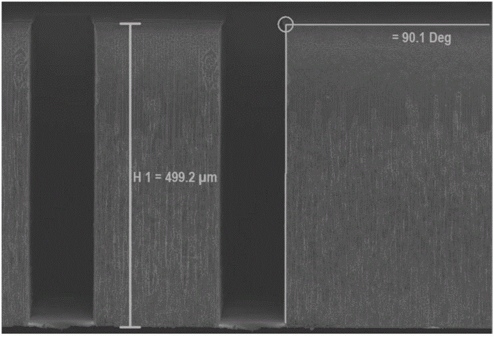
[0033] (1) Prepare an 8 μm thick patterned photoresist mask on the surface of a 500 μm thick silicon wafer.

[0034] (2) Perform deep inductively coupled plasma dry etching on the silicon wafer, including four etching stages.

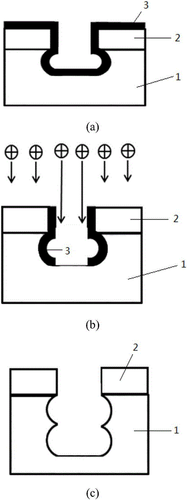
[0035] (2-1) The first etching stage: three steps of passivation, bombardment and etching are used for 400 times of alternate cycle processing, and the etching depth is 180 μm. The schematic diagram of the process flow of a single cycle is as follows: figure 1 shown.

[0036] Among them, the process parameters of the passivation step are: ion source power 2000W, lower electrode power 0W, cavity air pressure 90mtorr, C 4 f 8 Flow 250sccm, SF 6 The flow rate is 20sccm, and the time is 0.40s.

[0037] The process parameters of the bombardment step are: ion source power 3000W, lower electrode power 75W, cavity air pressure 30mTorr, C 4 f 8 Flow 20sccm, SF 6 The flow rate is 250...

Embodiment 2

[0053] The deep silicon etching method comprises the following steps:

[0054] (1) Prepare a 5 μm thick patterned photoresist mask on the surface of a 350 μm thick silicon wafer.

[0055] (2) Perform deep inductively coupled plasma dry etching on the silicon wafer, including four etching stages.

[0056] (2-1) The first etching stage: three steps of passivation, bombardment and etching are used for 400 times of alternating cycle processing, and the etching depth is 120 μm.

[0057] Among them, the process parameters of the passivation step are: ion source power 1500W, lower electrode power 0W, cavity air pressure 50mTorr, C 4 f 8 Flow 150sccm, SF 6 The flow rate is 0sccm, and the etching time is 0.375s.

[0058] The process parameters of the bombardment step are: ion source power 2000W, lower electrode power 50W, cavity air pressure 15mTorr, C 4 f 8 Flow 0sccm, SF 6 The flow rate is 100sccm, and the etching time is 0.6s.

[0059] The process parameters of the etching s...


PUM

PropertyMeasurementUnit
depthaaaaaaaaaa
depthaaaaaaaaaa
depthaaaaaaaaaa

Abstract

The invention discloses a deep silicon etching method which comprises the following steps: (1) preparing a graphic photoresist mask on a silicon chip surface; (2) performing deep inductively coupled plasma dry etching of the silicon chip, wherein the etching is divided into several phases, each etching phase is completed in a inductively coupled plasma machine, and is completed through alternate circular processing of three steps of passivation, bombardment, and etching, and with the increase of the etching depth, the bombardment intensity in the bombardment step of each etching phase increases gradually. The method of the invention effectively solves the problems of difficult control of sidewall verticality and roughness, and difficult realization of large etching depth in the prior art, both improves the etching efficiency and increases the selection ratio or photoresist, and is high in etching groove sidewall verticality, low in roughness, and large in etching depth.

Description

technical field [0001] The invention belongs to the technical field of plasma processing, and more specifically relates to a deep silicon etching method. Background technique [0002] Micro-electro-mechanical systems (MEMS) are more and more widely used in the fields of automobiles and consumer electronics, and the development of MEMS technology based on microelectronics technology is particularly rapid. The introduction of high-aspect-ratio silicon etch techniques into microelectronics processes has enabled a range of novel sensor and actuator structures. Compared with the surface processing technology, the bulk silicon structure obtained by the deep silicon etching process has a larger movable sensitive mass, a larger detection capacitance, and higher performance indicators such as device resolution and sensitivity. However, as a key step in the processing of bulk silicon MEMS devices, it is difficult to control the verticality and roughness of the sidewalls in the existi...

Claims


Application Information

Patent Timeline
Patent Type & Authority Patents(China)
IPC IPC(8): B81C1/00
Inventor 涂良成伍文杰范继刘金全罗俊
Owner HUAZHONG UNIV OF SCI & TECH
Learn More