Display panel assembly and adjusting method thereof, and display device
A technology of a display panel and an adjustment method, which is applied to static indicators, nonlinear optics, instruments, etc., can solve problems such as the realization of a narrow frame, which is disadvantageous for panel cost control, and a large fan-out area, and achieves reduced height, uniform brightness, The effect of impedance difference cancellation
- Summary
- Abstract
- Description
- Claims
- Application Information
AI Technical Summary
Problems solved by technology
Method used
Image

Examples
Embodiment 1
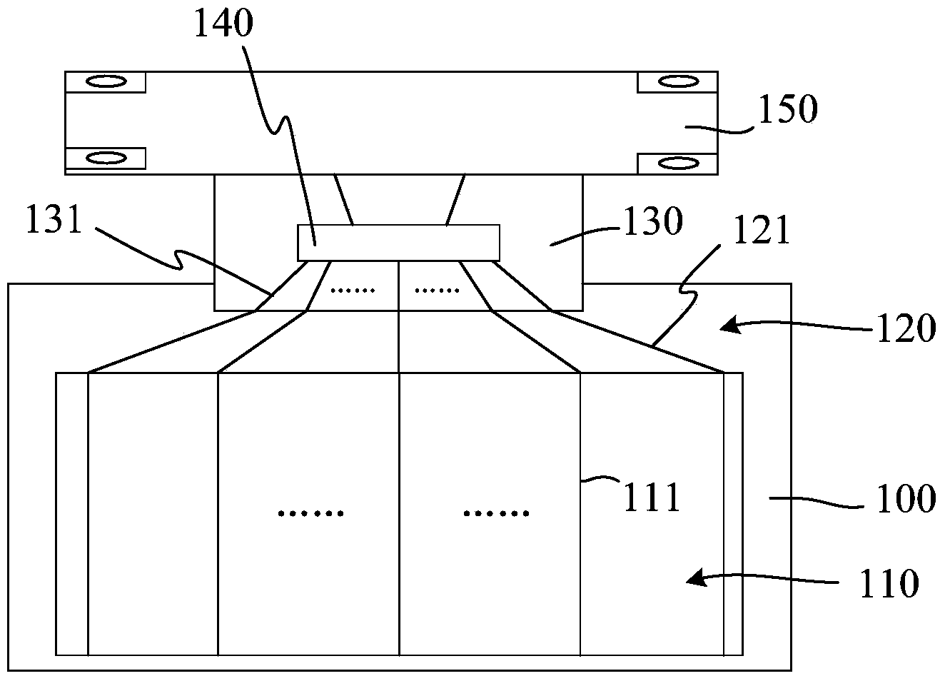
[0036] Such as image 3 Shown is a liquid crystal display panel assembly provided in this embodiment, which includes: a display panel 100 , a display area 110 set on the display panel 100 , a fan-out area 120 set on the display panel 100 , and a display area 110 set on the display panel 100 . The package at the edge has a film-on-chip 130 of a driver IC 140 and a PCB 150 .
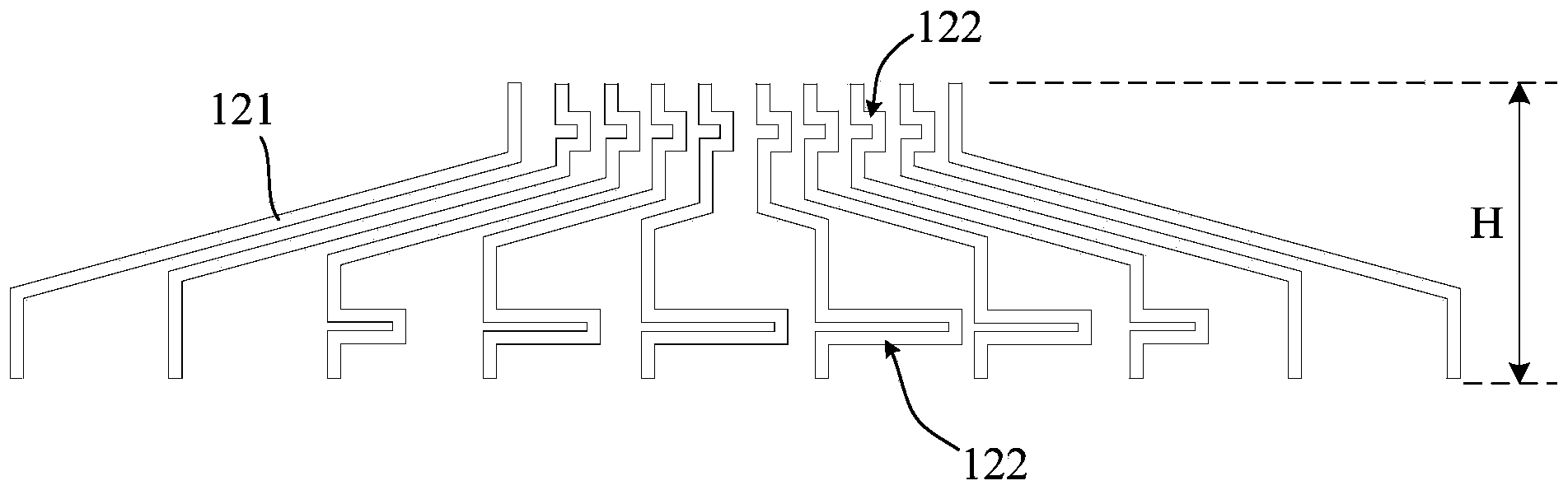
[0037] Wherein, the display area 110 is provided with a plurality of first data lines 111, and the fan-out area 120 is provided with a plurality of second data lines 121 with various lengths connected to the first data lines 111; The closer the area, the shorter the length of the second data line 121, and the second data line 121 is laid according to a straight line, so as to reduce the width of the edge of the display panel 100 as much as possible, which better realizes the display device. narrow bezel design. The film-on-chip 130 is used to connect the display panel 100 and the PCB 150. The driver IC 1...
Embodiment 2
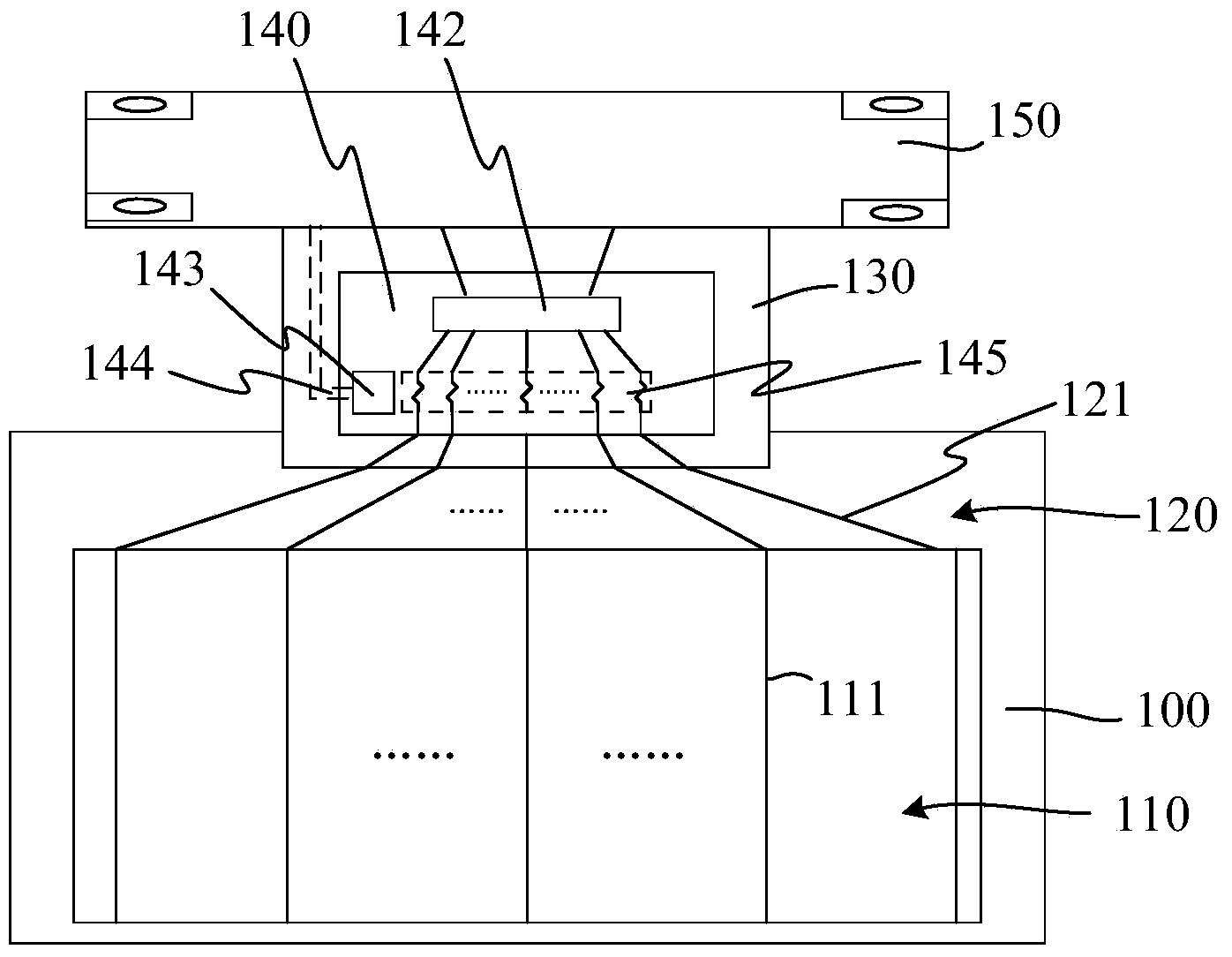
[0044] In this embodiment, on the basis of the first embodiment above, the adjustable resistance group 145 is grouped again, that is to say, the adjustable resistance group includes a plurality of sub-adjustable resistance groups, which can be adjusted for each sub-resistance group. A group of sub-resistor groups can be adjusted to a uniform resistance value, so that it is not necessary to set different resistors for the output of each functional circuit, and only need to use a group of resistors with the same resistance value to reduce the connection (the output terminal of the functional circuit to the first One data line 111) between the impedance difference is enough, such a setting can basically eliminate the signal delay or the signal delay is very weak, and the impact on the display effect can be ignored. This setting method makes the cost can be greatly reduced decrease.
Embodiment 3
[0046] Such as Figure 4 As shown, the difference from the first embodiment is that the present embodiment can directly integrate the resistor 144 in the driver IC 140, the third data line 131 is coupled to the output end of the driver IC 140 through the resistor 144, and the third data line 131 is connected to the panel on the panel. The second data line connection of the fan-out area. This method does not require a special control circuit to control the resistance, but the driver IC of this method can only be applied to one type of panel. Likewise, a plurality of resistor groups with the same resistance value can be used to form a group of resistor groups, and multiple groups of resistor groups with different resistance values can be integrated in the driving IC 140 . In this way, it is not necessary to set different resistors for each output terminal of the driver IC140, it is only necessary to reduce the impedance difference through a group of resistors with the same re...
PUM
 Abstract
Description
Claims
Application Information
 - R&D
- Intellectual Property
- Life Sciences
- Materials
- Tech Scout
- Unparalleled Data Quality
- Higher Quality Content
- 60% Fewer Hallucinations
Browse by: Latest US Patents, China's latest patents, Technical Efficacy Thesaurus, Application Domain, Technology Topic, Popular Technical Reports.
© 2025 PatSnap. All rights reserved.Legal|Privacy policy|Modern Slavery Act Transparency Statement|Sitemap|About US| Contact US: help@patsnap.com