Three-dimensional paper-based microfluidics and manufacture method thereof

A technology of microfluidic chip and manufacturing method, which is applied in the direction of analyzing materials and instruments, and can solve the problems of inability to carry out the analysis process, reduce the fluid flow rate, and pollute the test results, etc., and achieve the easy operation, easy acquisition, and simple manufacturing process of the manufacturing process Effect

Inactive Publication Date: 2014-06-18
DALIAN INST OF CHEM PHYSICS CHINESE ACAD OF SCI
View PDF4 Cites 16 Cited by
  • Summary
  • Abstract
  • Description
  • Claims
  • Application Information

AI Technical Summary

Problems solved by technology

However, the double-sided adhesive or spray glue used in the above two methods will reduce the flow rate of the fluid in the hydrophilic channel in the paper chip on the one hand, and increase the time it takes for the fluid to penetrate the entire three-dimensional paper chip. On-site detection of test results is extremely unfavorable; on the other hand, double-sided adhesive or spray glue will be dissolved by organic solvents such as methanol, ethanol, ethyl acetate, etc., if the pretreatment reagent or detection reagent of the chip contains organic solvent, It will dissolve the adhesive between the layers of the chip, which will damage the paper chip and make the analysis process impossible
In addition, the detection reagent or pretreatment reagent circulating in the channel of the chip directly contacts the adhesive, which may also cause contamination and make the detection result inaccurate
Folding and pressing method, the whole chip is made on a piece of paper, and then completed by folding and pressing. The layers of paper chips are kept in contact with each other. This auxiliary clip is generally made of metal or other rigid plastics. The production process is cumbersome and the cost is high. It should also be different according to the different design structures of the chips.

Method used


Image

  • Three-dimensional paper-based microfluidics and manufacture method thereof
  • Three-dimensional paper-based microfluidics and manufacture method thereof

Examples


Embodiment 1

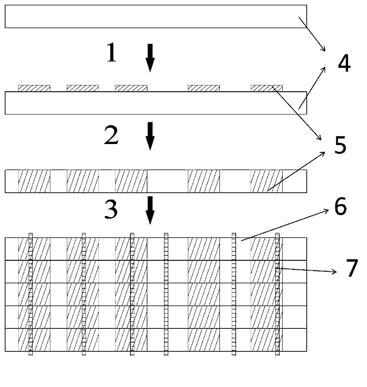
[0021] Example 1: Making a three-dimensional paper chip using the bookbinding method

[0022] Use drawing software to design the required chip design pattern on the computer, then print the chip design pattern on the filter paper with a wax spray printer, and then put the filter paper printed with wax on the surface into an oven at 150 degrees to bake for 3 minutes (this process The wax will melt and permeate the filter paper), forming a hydrophilic / hydrophobic interphase area, and then take it out to cool, and then get a two-dimensional paper microfluidic chip. Stack the six-layer two-dimensional paper microfluidic chip, and then use a stapler to staple the staples into the designed binding position of the chip to obtain a three-dimensional paper chip. The specific flow chart is as figure 1 Shown (includes three main steps: 1) wax spray printing; 2) cutting and baking; 3) lamination and binding. )

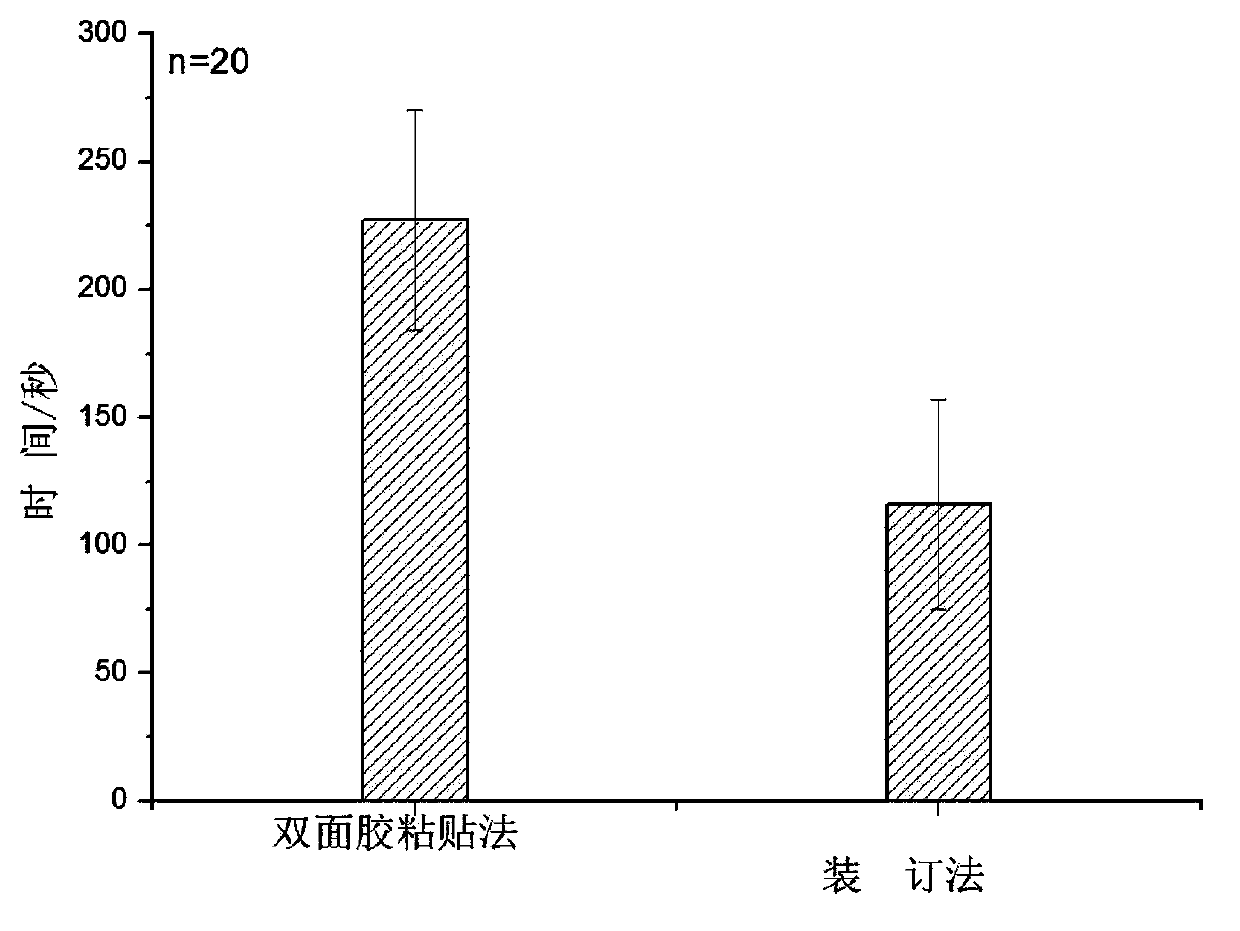
[0023] This fabrication method is simple, fast, and low-cost, which is ver...


PUM


Abstract

The invention provides three-dimensional paper-based microfluidics and a manufacture method thereof. The three-dimensional paper-based microfluidics is formed by overlapping and bookbinding of two-dimensional paper-based microfluidics. The manufacture method comprises the steps: designing a required chip pattern by drawing software, then printing wax onto the surface of a paper material with a printer, putting the printed paper material into a high-temperature container, baking, then taking out, and cooling to obtain the two-dimensional paper-based microfluidics; and then overlapping the two-dimensional paper-based microfluidics according to a designed way, next bookbinding the overlapped two-dimensional paper-based microfluidics together by a bookbinding device, and thus obtaining the three-dimensional paper-based microfluidics. The manufacture method has the advantages of simple operation, low cost and speediness, and has commercialization prospects.

Description

technical field [0001] The invention relates to the development of biochemical analysis products, and in particular provides a three-dimensional paper microfluidic chip and a manufacturing method thereof. Background technique [0002] Paper-based Microfluidics, referred to as paper chip, is a microfluidic chip that uses paper materials (such as filter paper, chromatographic paper, nitrocellulose membrane, etc.) as the chip production platform and biochemical analysis platform. In the paper chip system, the hydrophobic material divides the hydrophilic paper material into the area between the hydrophilic and hydrophobic phases to form a paper channel, and integrates basic operation units such as sampling, separation, reaction, and detection, and runs through the whole with controllable fluid. The system realizes the analysis function of the routine laboratory. In early 2007, the Whitesides group at Harvard University made paper chips for the first time and proposed this conce...

Claims


Application Information

Patent Timeline
Patent Type & Authority Applications(China)
IPC IPC(8): G01N35/00
Inventor 杜昱光肖良品林炳承刘启顺
Owner DALIAN INST OF CHEM PHYSICS CHINESE ACAD OF SCI
Why Eureka
Try Eureka