A flexible display substrate motherboard and a method for manufacturing the flexible display substrate

A flexible display and manufacturing method technology, applied in the direction of final product manufacturing, sustainable manufacturing/processing, semiconductor/solid-state device manufacturing, etc., can solve the problem of limited beam area, uneven peeling of flexible substrates and the carrier substrate, and damage to display elements And other issues

Active Publication Date: 2017-01-18
BOE TECH GRP CO LTD
View PDF3 Cites 0 Cited by
  • Summary
  • Abstract
  • Description
  • Claims
  • Application Information

AI Technical Summary

Problems solved by technology

[0004] However, when the laser beam is used for the lift-off process, although the intensity and focus depth of the laser beam are controlled, since the flexible substrate and each pattern layer of the display element formed on the flexible substrate are very thin, the light of the laser beam is still very thin. Will inevitably damage the display components
In addition, due to the limited beam area of ​​the laser beam, the flexible substrate and the hard carrier substrate need to be gradually peeled off by moving the laser beam during peeling, which will lead to uneven peeling of the flexible substrate and the carrier substrate. Phenomenon

Method used


Image

  • A flexible display substrate motherboard and a method for manufacturing the flexible display substrate
  • A flexible display substrate motherboard and a method for manufacturing the flexible display substrate
  • A flexible display substrate motherboard and a method for manufacturing the flexible display substrate

Examples


Embodiment Construction

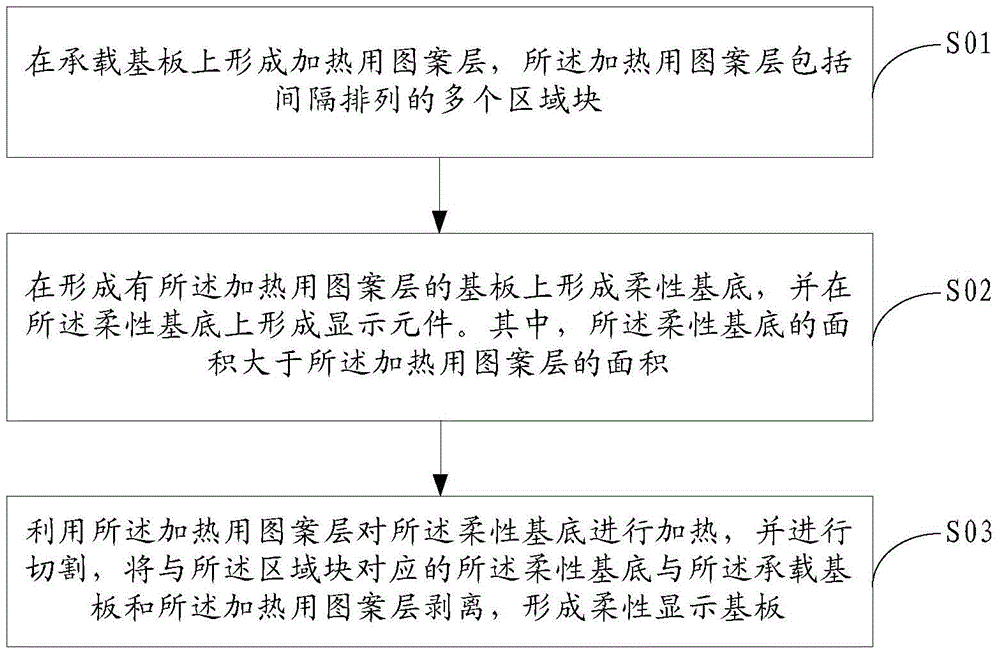
[0052] The following will clearly and completely describe the technical solutions in the embodiments of the present invention with reference to the accompanying drawings in the embodiments of the present invention. Obviously, the described embodiments are only some, not all, embodiments of the present invention. Based on the embodiments of the present invention, all other embodiments obtained by persons of ordinary skill in the art without making creative efforts belong to the protection scope of the present invention.

[0053] An embodiment of the present invention provides a method for manufacturing a flexible display substrate, such as figure 1 As shown, the method includes the following steps:

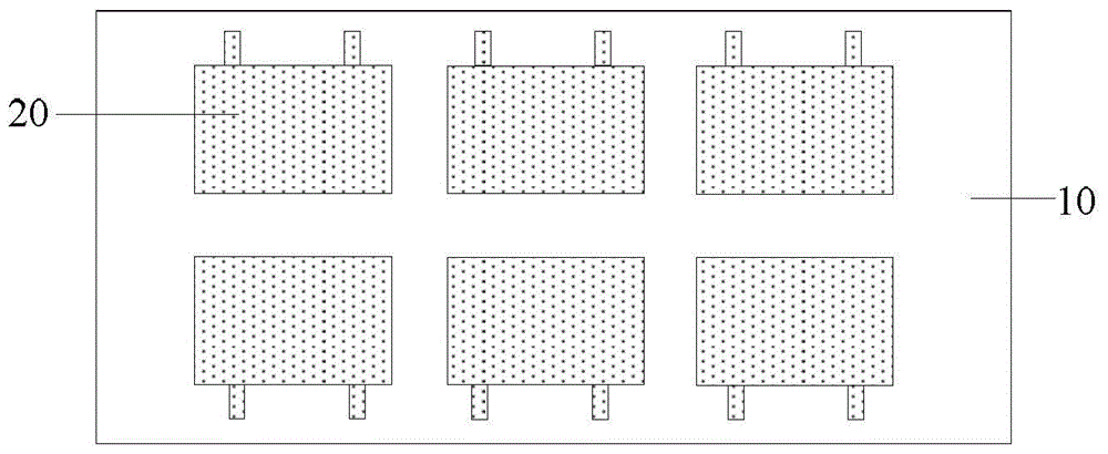
[0054] S01. Form a patterned layer for heating on a carrier substrate, where the patterned layer for heating includes a plurality of area blocks arranged at intervals.

[0055] S02. Form a flexible base on the substrate on which the heating pattern layer is formed, and form a disp...


PUM


Abstract

Embodiments of the present invention provide a flexible display substrate motherboard and a method for manufacturing the flexible display substrate, which relate to the field of display technology and can avoid damage to display elements on the flexible substrate when the flexible substrate is separated from the carrier substrate, and avoid The phenomenon of uneven separation; the method includes: forming a patterned layer for heating on a carrier substrate, the patterned layer for heating includes a plurality of area blocks arranged at intervals; forming a flexible base on the substrate formed with a patterned layer for heating, and A display element is formed on the substrate; wherein, the area of ​​the flexible substrate is larger than the area of ​​the heating pattern layer; the flexible substrate is heated by the heating pattern layer and cut, and the supporting substrate corresponding to the area block and the flexible substrate are peeled off to form a flexible substrate. Displays the substrate. It is used in the manufacture of a flexible display substrate that needs to avoid damage to display elements on the flexible substrate and avoid uneven separation when the flexible substrate and the carrier substrate are separated.

Description

technical field [0001] The invention relates to the field of display technology, in particular to a flexible display substrate motherboard and a method for manufacturing the flexible display substrate. Background technique [0002] Flexible display technology has developed rapidly in recent years, which has led to great progress in flexible displays from screen size to display quality. Whether it is the cathode ray tube (Cathode Ray Tube, referred to as CRT) that is on the verge of disappearing, or the current mainstream liquid crystal display (Liquid Crystal Display, referred to as LCD), they are essentially traditional rigid displays. Compared with traditional rigid displays, flexible displays have many advantages, such as impact resistance, strong shock resistance, light weight, small size, and more convenient to carry. [0003] Flexible displays can be mainly divided into three types: electronic paper (flexible electrophoretic display), flexible organic light-emitting d...

Claims


Application Information

Patent Timeline
Patent Type & Authority Patents(China)
IPC IPC(8): H01L27/12H01L27/32H01L21/683H01L21/78
CPCH01L21/78H01L29/78603H01L21/76Y02E10/549H01L27/1218Y02P70/50H10K59/00H10K59/12H10K77/111H10K50/824H10K50/87H10K2102/311H10K71/00H10K59/1201H01L27/12G02F1/133305G02F1/133514G02F1/1368H01L27/1262
Inventor 谢明哲谢春燕刘陆
Owner BOE TECH GRP CO LTD
Why Eureka
Try Eureka