Semiconductor device
一种半导体、器件的技术,应用在半导体器件领域,能够解决毁坏半导体器件等问题,达到提高耐受性、减小导通电压的增大、减小电压降的效果
- Summary
- Abstract
- Description
- Claims
- Application Information
AI Technical Summary
Problems solved by technology
Method used
Image


Examples
no. 1 example )
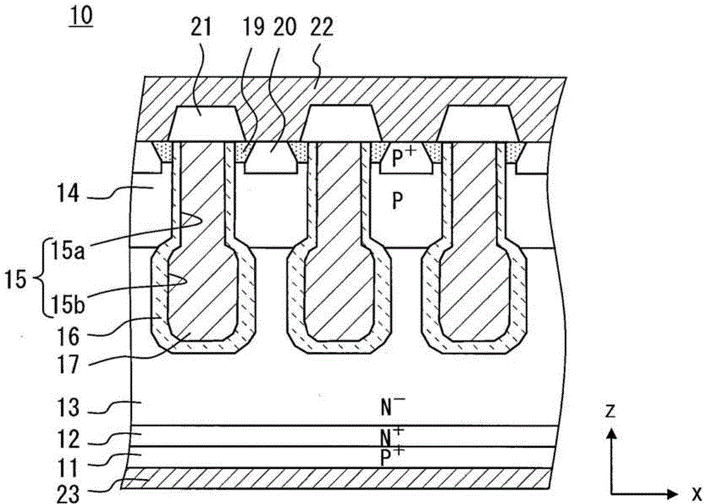
[0060] First, refer to figure 1 and figure 2 The structure of the semiconductor device 10 according to the present embodiment will be described.
[0061] Such as figure 1 As shown, N with a predetermined thickness in the z direction + type buffer layer 12 formed on the P + type collector layer 11 on the surface, the P + The type collector layer 11 is formed along the x-y plane and has a predetermined thickness in the x direction. N having an impurity concentration lower than that of the buffer layer 12 - Type drift layer 13 is formed on the surface of buffer layer 12 . P-type base layer 14 is formed on the surface of drift layer 13 . That is, collector layer 11 , buffer layer 12 , and drift layer 13 are stacked in this order.
[0062] A plurality of trenches 15 penetrating the base layer 14 and reaching the drift layer 13 extend in the y direction to form a stripe pattern. According to the present embodiment, trenches 15 are repeatedly formed at a regular gate pitch ...
no. 2 example )
[0084] In the first embodiment, the length D of the communicating portion 18a in the z direction 1 is about 3.0 μm, and the length D of the bottom 18b in the z direction 2 is about 2.0 μm. In contrast, according to this embodiment, the length D 1 is approximately 2.4µm, while the length D 2 is about 1.6µm (is the length of the first embodiment D 2 0.8 times), so that the base layer 14, the emitter layer 19, and the base layer 14 form the base contact layer 20 from the surface at depths 0.8 times those of the first embodiment.
[0085] Since the structures other than the above-mentioned dimensions are the same as those of the first embodiment, detailed descriptions of other structures are omitted. In addition, regarding the advantages, because factors other than the conduction voltage are compared with the dependence of D1, D2, the base layer 14, the emitter layer 19, and the depth at which the base layer 14 forms the base contact layer 20 from the surface The turn-on volt...
no. 3 example )
[0089] In the foregoing embodiments, the base layer 14 is located between adjacent gate trenches 18 and between adjacent emitter layers 19 . On the contrary, according to this embodiment, if Figure 8 As shown, the emitter layer 19 is continuous in the x-direction between adjacent trench gates 18 .
[0090] According to the present embodiment, emitter layer 19 is formed in the surface portion of base layer 14 and is continuous in the x direction between adjacent trench gates 18 . Like in the first embodiment, the length “C” of the base contact layer 20 is about 0.8 μm in the x direction and is spaced apart from the trench gate 18 . The thickness of the base contact layer 20 in the z direction from the base layer 14 is the same as the thickness of the emitter layer 19 . In this way, the emitter layers 19 and the base contact layers 20 are alternately arranged in the y-direction and extend from the surface of the base layer 14 to the same depth.
[0091] According to the pres...
PUM
 Abstract
Description
Claims
Application Information
 - R&D
- Intellectual Property
- Life Sciences
- Materials
- Tech Scout
- Unparalleled Data Quality
- Higher Quality Content
- 60% Fewer Hallucinations
Browse by: Latest US Patents, China's latest patents, Technical Efficacy Thesaurus, Application Domain, Technology Topic, Popular Technical Reports.
© 2025 PatSnap. All rights reserved.Legal|Privacy policy|Modern Slavery Act Transparency Statement|Sitemap|About US| Contact US: help@patsnap.com