Transparent conductive substrate and touch panel having the same

A transparent, substrate technology, applied to the conductive layer on the insulating carrier, the input/output process of data processing, optics, etc., to achieve the effect of low manufacturing cost, fast coating speed, and excellent productivity

Inactive Publication Date: 2014-04-09
SAMSUNG CORNING PRECISION MATERIALS CO LTD
View PDF7 Cites 5 Cited by
  • Summary
  • Abstract
  • Description
  • Claims
  • Application Information

AI Technical Summary

Problems solved by technology

In this case, however, the pattern can be seen visually, even after placing the index-matching layer between the window cover glass and the transparent conductive film, which is problematic

Method used


Image

  • Transparent conductive substrate and touch panel having the same
  • Transparent conductive substrate and touch panel having the same

Examples


Embodiment 1

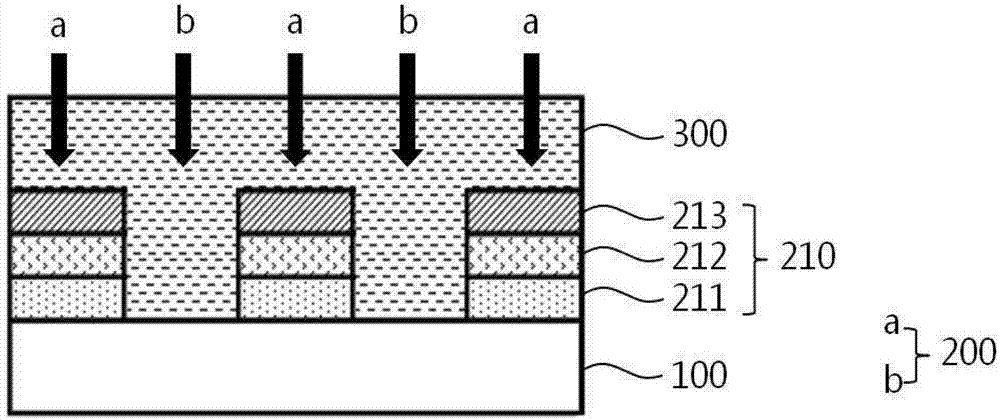
[0052] The transparent conductive substrate according to Example 1 includes a glass substrate on which is formed a glass substrate having a thickness of 31 nm and made of Nb 2 o 5 The first film made, on the first film, a planarization layer with a thickness of 5 nm and made of ZnO is formed, on the planarization layer, a metal film with a thickness of 10 nm and made of Ag is formed, on the metal film, a metal film with An anti-oxidation layer with a thickness of 5 nm and made of ZnO, and an anti-oxidation layer with a thickness of 31 nm and made of Nb 2 o 5 A second film was produced and a resin layer having a thickness of 5 μm was formed on the second film. Here, the resin layer was formed using Samyang EMS SOC3006U resin.

Embodiment 2

[0054] Except for the first film by Ta 2 o 5 made and has a thickness of 35nm, and the second film is made of Ta 2 o 5 The transparent conductive substrate according to Example 2 has the same configuration as Example 1 except that it is made and has a thickness of 36 nm.


PUM

PropertyMeasurementUnit
thicknessaaaaaaaaaa
thicknessaaaaaaaaaa
thicknessaaaaaaaaaa

Abstract

A transparent conductive substrate used for the detection of a touched position in a touch screen panel and a touch panel having the same. The transparent conductive substrate includes a base substrate, a transparent conductive layer formed on the base substrate, the transparent conductive layer including a pattern part which includes a transparent conductive film coating the base substrate and a non-pattern part through which the base substrate is exposed, and a polymer resin layer containing a resin that has a refractive index from 1.4 to 1.6, the polymer resin layer being formed on the transparent conductive layer while filling the non-pattern part, the thickness of the polymer resin layer from the pattern part ranging from 1 to 1000 [mu]m. The transparent conductive film includes a first thin film on the base substrate, a metal thin film on the first thin film, and a second thin film on the metal thin film.

Description

[0001] Cross References to Related Applications [0002] This application claims priority from Korean Patent Application No. 10-2012-0108927 filed on Sep. 28, 2012, the entire contents of which are hereby incorporated by reference in all respects. technical field [0003] The present invention relates to a transparent conductive substrate and a touch panel having the same, and more particularly, to a transparent conductive substrate for detecting a contact position in a touch screen panel (TSP) and a touch panel having the substrate. Background technique [0004] Generally, a touch panel refers to a device placed on the surface of a display device (such as a cathode ray tube (CRT), a liquid crystal display (LCD), a plasma display panel (PDP), or an electroluminescent (EL) device, etc.), so that the user While displaying the device screen, when the touch panel is touched with a finger or an input device such as a stylus pen, a signal may be output. Recently, touch panels are...

Claims


Application Information

Patent Timeline
Patent Type & Authority Applications(China)
IPC IPC(8): G06F3/041
CPCG06F3/041G02F1/13338G06F2203/04103G06F3/0443G06F3/0412G06F2203/04102G06F3/0448H01B5/14
Inventor 金义洙朴承元
Owner SAMSUNG CORNING PRECISION MATERIALS CO LTD
Why Eureka
Try Eureka