Universal device and method for protocol conversion
A protocol conversion and protocol data technology, applied in the field of virtual simulation experiment, can solve the problems of low conversion efficiency and conversion accuracy, and achieve the effect of improving conversion efficiency and conversion accuracy
- Summary
- Abstract
- Description
- Claims
- Application Information
AI Technical Summary
Problems solved by technology
Method used
Image
Examples
specific Embodiment approach 1
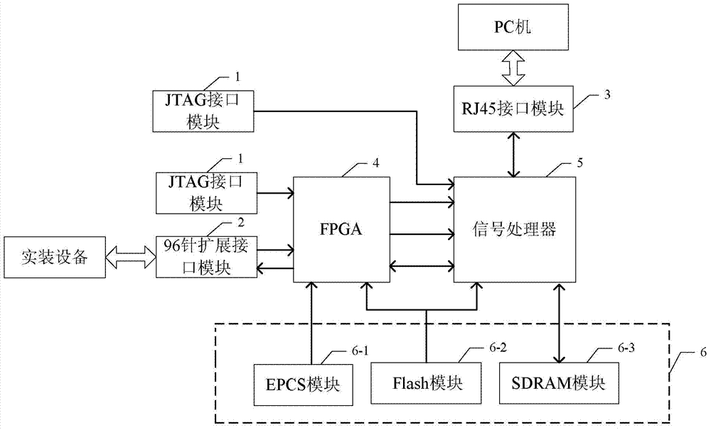
[0047] Specific implementation mode one: see figure 1 Describe the present embodiment, a kind of general protocol conversion device described in the present embodiment, it comprises two JTAG interface modules 1, 96 needle extension interface modules 2, RJ45 interface module 3, FPGA4, signal processor 5 and memory 6,
[0048] The burning program signal output end of one of the JTAG interface modules 1 is connected to the FPGA4 burning program signal input end, and the burning program signal output end of the other JTAG interface module 1 is connected to the signal processor 5 burning program signal input end connect,
[0049]The uplink protocol data signal output end of the 96-pin expansion interface module 2 is connected to the FPGA4 uplink protocol data signal input end, and the downlink protocol data signal input end of the 96-pin expansion interface module 2 is connected to the FPGA4 downlink protocol data signal output end,
[0050] The interrupt signal output end of FPGA...
specific Embodiment approach 2
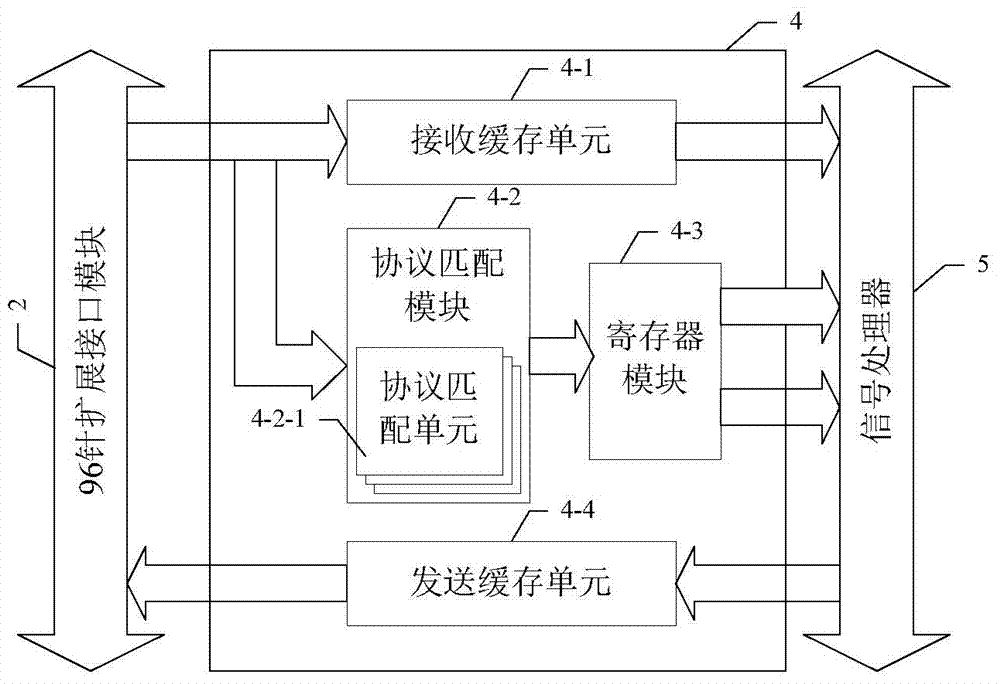
[0052] Specific implementation mode two: see figure 1 and 2 Describe this embodiment, the difference between this embodiment and a kind of general protocol conversion device described in the specific embodiment one is that the FPGA4 includes a receiving buffer unit 4-1, a protocol matching module 4-2, a register module 4- 3 and transmit buffer unit 4-4,
[0053] The data signal input end of the described receiving buffer unit 4-1 is connected with the protocol matching module 4-2 data signal input end as the FPGA4 uplink protocol data signal input end, and the uplink protocol data signal input end of the receiving buffer unit 4-1 and Sending cache unit 4-4 downlink protocol data signal input is connected as the up and down protocol data input and output terminals of FPGA4 and the up and down protocol data input and output terminals of signal processor 5,
[0054] The data signal output end of the sending buffer unit 4-4 is used as the FPGA4 downlink protocol data signal outp...
specific Embodiment approach 3
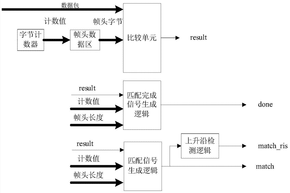
[0058] Specific implementation mode three: see figure 1 , 2 and 3 illustrate this embodiment, the difference between this embodiment and the general-purpose protocol conversion device described in the third embodiment is that the acquisition process of the protocol matching module 4-2 is that 64 protocol matching units 4 -2-1 forming a protocol matching unit array, the protocol matching unit array is added with auxiliary function logic, and finally a protocol matching module 4-2 is obtained;
[0059] The protocol matching unit 4-2-1 is used to perform protocol matching on the received uplink protocol data signal, and send the matching result to the matching result signal input end of the signal processor 5,
[0060] The auxiliary function logic includes a 64-bit AND module, a 64-bit OR module, a 64-bit priority encoder and an 8-bit trigger,
[0061] The 64-bit priority encoder encodes the priority of match_ris, and match_ris is the match occurrence signal,
[0062] The 64-b...
PUM
 Abstract
Description
Claims
Application Information
 - R&D
- Intellectual Property
- Life Sciences
- Materials
- Tech Scout
- Unparalleled Data Quality
- Higher Quality Content
- 60% Fewer Hallucinations
Browse by: Latest US Patents, China's latest patents, Technical Efficacy Thesaurus, Application Domain, Technology Topic, Popular Technical Reports.
© 2025 PatSnap. All rights reserved.Legal|Privacy policy|Modern Slavery Act Transparency Statement|Sitemap|About US| Contact US: help@patsnap.com


