Live line and zero line identifying/converting circuit for charger
A technology for converting circuits and chargers, which is applied to battery circuit devices, current collectors, circuit devices, etc.
- Summary
- Abstract
- Description
- Claims
- Application Information
AI Technical Summary
Problems solved by technology
Method used
Image
Examples
Embodiment 1
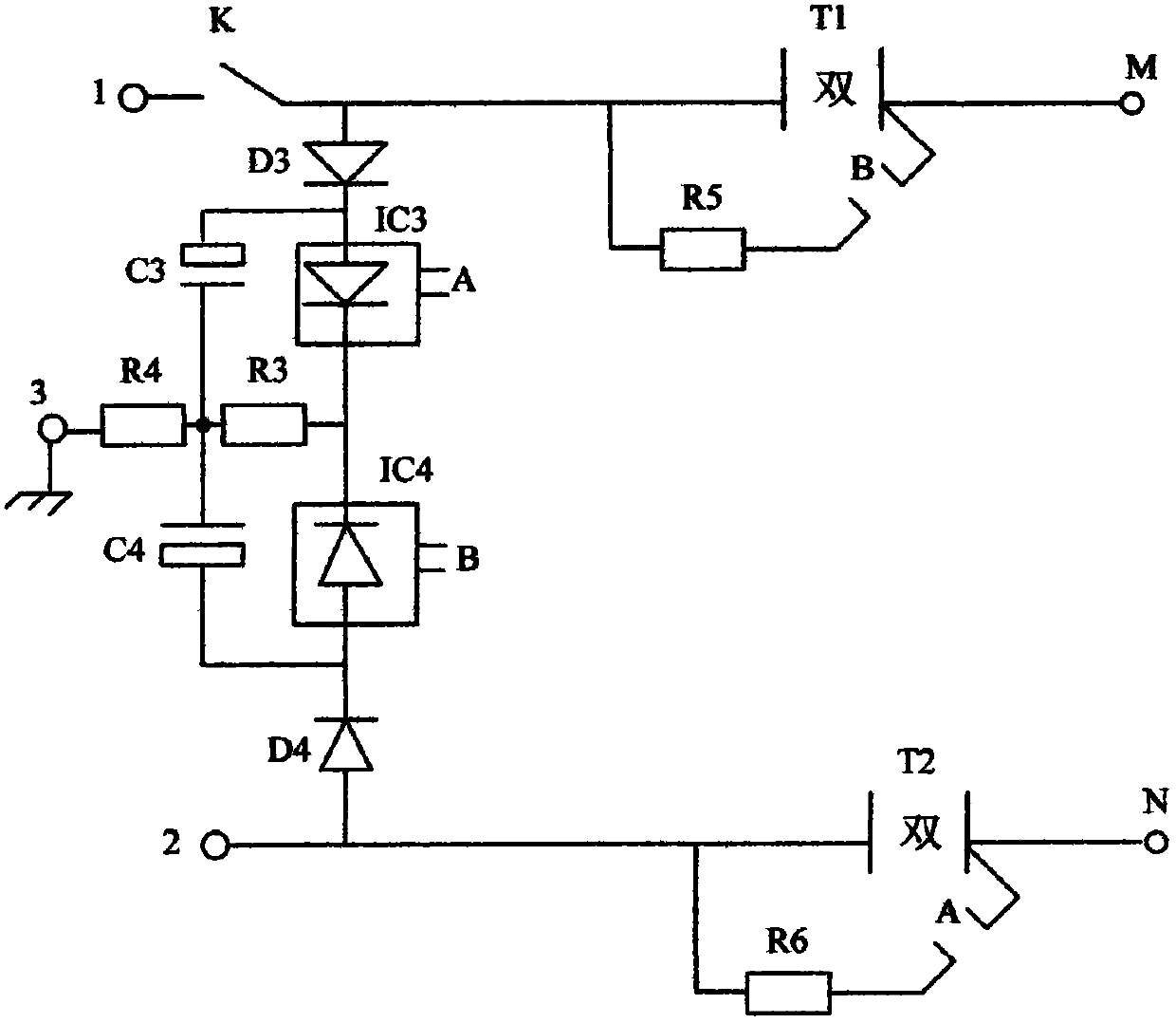
[0020] The charger of this embodiment uses live wire and neutral wire to identify conversion circuit, such as figure 1 , including: the third diode D3, the fourth diode D4, the third optocoupler thyristor IC3, the fourth optocoupler thyristor IC4, the third filter capacitor C3, the fourth filter capacitor C4, the third resistor R3, the fourth resistor R4, mains input and ground wire;
[0021] The charger includes a first bidirectional thyristor T1 and a second bidirectional thyristor T2, and the two bidirectional thyristors are switches or charging isolation circuits of the charger;
[0022] One terminal 1 of the AC input terminal is respectively connected to the anode of the third diode D3, one terminal of the control switch of the fourth optocoupler thyristor IC4, and the second anode of the first bidirectional thyristor T1; the terminal of the third diode D3 The negative pole is respectively connected to the positive pole of the third filter capacitor C3 and the positive p...
Embodiment 2
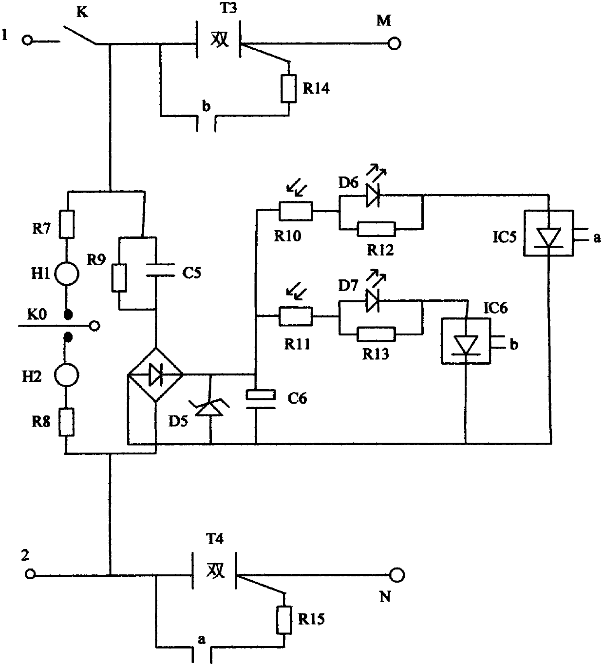
[0030] The charger in this embodiment uses live wire and neutral wire identification circuit, such as figure 2 shown, including:
[0031] Bridge pile, seventh, eighth, ninth, twelfth, thirteenth, fourteenth, fifteenth resistor R7, R8, R9, R12, R13, R14, R15, tenth, eleventh photoresistor R10 . Neon tube H2, normally open switch K0, fifth capacitor C5; wherein, the sixth LED light-emitting diode D6, the tenth photoresistor R10 and the first neon tube H1 are arranged together, the seventh LED light-emitting diode D7, the eleventh photoresistor R11 is set together with the second neon tube H2;
[0032] The charger includes a third triac T3 and a second triac T2;
[0033] One terminal 1 of the AC input terminal is respectively connected with one terminal of the seventh resistor R7, one terminal of the ninth resistor R9, one terminal of the fifth capacitor C5, one terminal of the control switch of the sixth optocoupler thyristor IC6, and one terminal of the third bidirectional ...
Embodiment 3
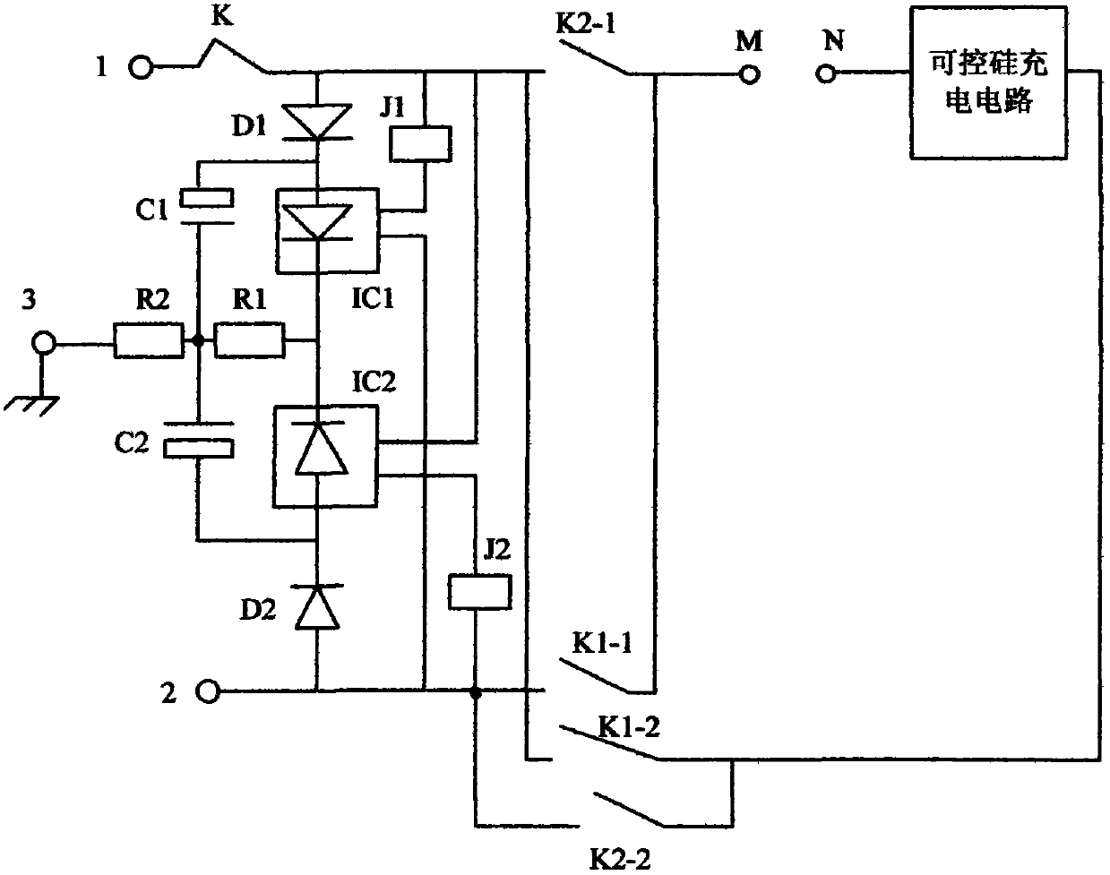
[0037] The charger in this embodiment uses live wire and neutral wire identification circuit, such as image 3 , including: first relay J1, second relay J2, first diode D1, second diode D2, first optocoupler thyristor IC1, second optocoupler thyristor IC2, first filter capacitor C1 , the second filter capacitor C2, the first resistor R1, the second resistor R2; mains input and ground wire;
[0038] The third switch K2-1, the first switch K1-1, the second switch K1-2, and the fourth switch K2-2; wherein, the first relay J1 controls the switching of the first switch K1-1 and the second switch K1-2 off, the second relay J2 controls the on-off of the third switch K2-1 and the fourth switch K2-2;
[0039] One end 1 of the AC input end is respectively connected with the anode of the first diode D1, one end of the coil of the first relay J1, one end of the control switch of the second optocoupler thyristor IC2, one end of the third switch K2-1, the second switch One end of K1-2 is ...
PUM
 Abstract
Description
Claims
Application Information
 - R&D
- Intellectual Property
- Life Sciences
- Materials
- Tech Scout
- Unparalleled Data Quality
- Higher Quality Content
- 60% Fewer Hallucinations
Browse by: Latest US Patents, China's latest patents, Technical Efficacy Thesaurus, Application Domain, Technology Topic, Popular Technical Reports.
© 2025 PatSnap. All rights reserved.Legal|Privacy policy|Modern Slavery Act Transparency Statement|Sitemap|About US| Contact US: help@patsnap.com


