Solar component with protective layer
A solar module with a protective layer technology, applied in the field of solar modules, can solve the problems of low recombination rate and reduced lifespan of minority carriers on the surface of silicon wafers, and achieve high conversion efficiency, optimized graphic design, and high adhesion
- Summary
- Abstract
- Description
- Claims
- Application Information
AI Technical Summary
Problems solved by technology
Method used
Image
Examples
Embodiment 1)
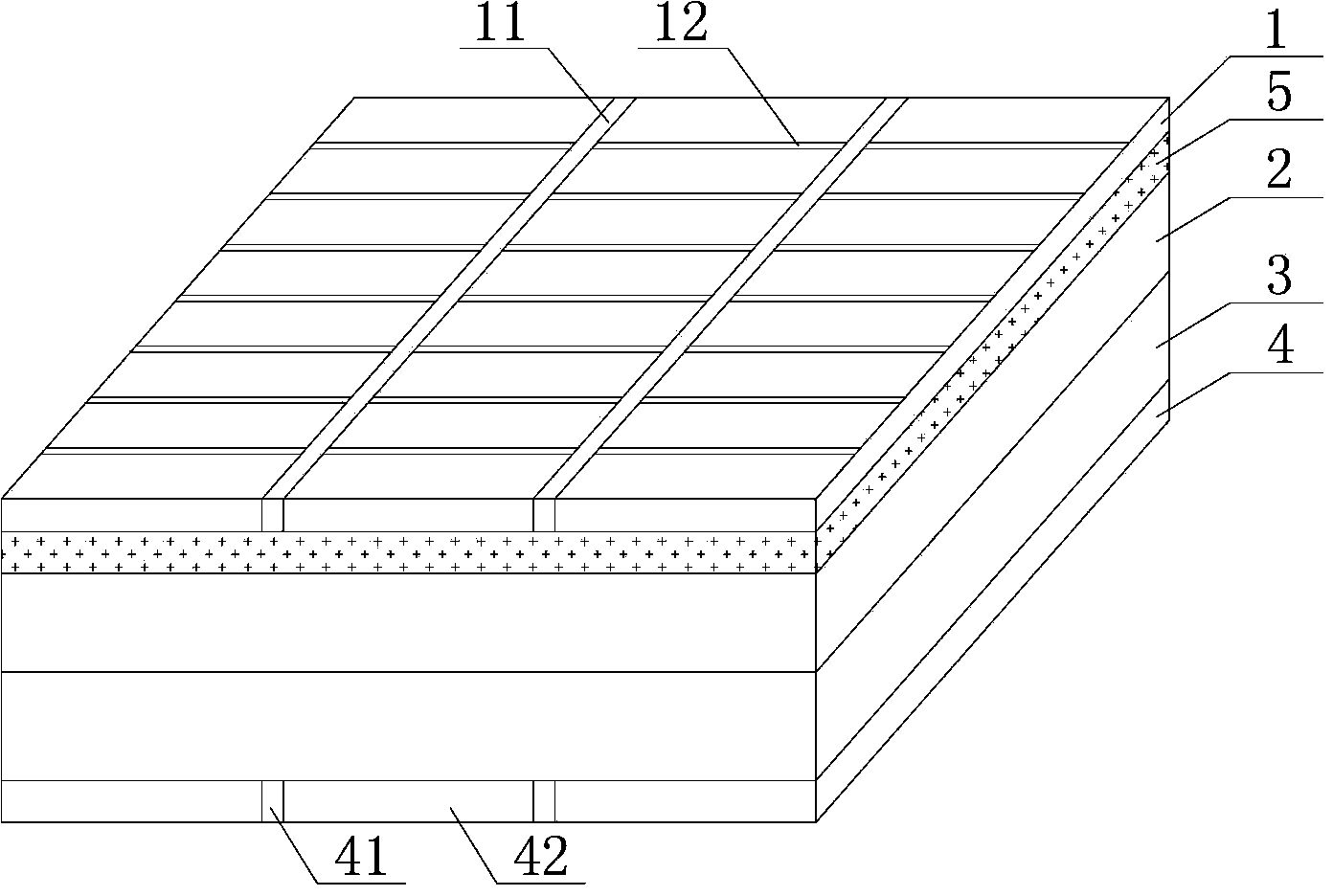
[0016] See figure 1 , the present invention has negative electrode layer 1, N-type silicon layer 2, P-type silicon layer 3, positive electrode layer 4 and anti-reflection film layer 5 stacked in sequence; negative electrode layer 1 and positive electrode 1 are both silver layers, and on the surface of negative electrode layer 1 There is a main grid 11 formed by screen pattern printing and sub-gates 12 perpendicular to the main grid 11 and equally spaced; the positive layer 4 has a back electrode 41 and a back electric field 42; the anti-reflection film layer 5 is a silicon nitride layer , the anti-reflection film layer 5 is disposed between the negative electrode layer 1 and the N-type silicon layer 2 .
PUM
 Abstract
Description
Claims
Application Information
 - R&D
- Intellectual Property
- Life Sciences
- Materials
- Tech Scout
- Unparalleled Data Quality
- Higher Quality Content
- 60% Fewer Hallucinations
Browse by: Latest US Patents, China's latest patents, Technical Efficacy Thesaurus, Application Domain, Technology Topic, Popular Technical Reports.
© 2025 PatSnap. All rights reserved.Legal|Privacy policy|Modern Slavery Act Transparency Statement|Sitemap|About US| Contact US: help@patsnap.com

