A trench structure charge compensation Schottky semiconductor device and its manufacturing method
A charge compensation, conductive semiconductor technology, used in semiconductor/solid-state device manufacturing, semiconductor devices, circuits, etc., can solve problems such as high on-resistance, cannot be used in high-voltage environments, and low forward turn-on voltage.
- Summary
- Abstract
- Description
- Claims
- Application Information
AI Technical Summary
Problems solved by technology
Method used
Image

Examples
Embodiment 1
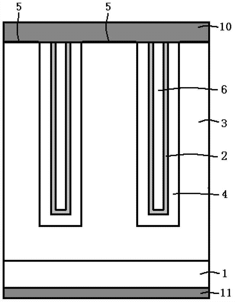
[0014] figure 1 It is a cross-sectional view of a trench structure charge compensation Schottky semiconductor device of the present invention, combined below figure 1 The semiconductor device of the present invention will be described in detail.
[0015] A Schottky semiconductor device, comprising: a substrate layer 1, which is an N conductivity type semiconductor silicon material, and the doping concentration of phosphorus atoms is 1E19 / CM 3 , on the lower surface of the substrate layer 1, the electrodes are drawn out through the lower surface metal layer 11; the first conductive semiconductor material 3, located on the substrate layer 1, is a semiconductor silicon material of N conductivity type, and the doping concentration of phosphorus atoms is 1E16 / CM 3 ; The second conductive semiconductor material 4, located near the inner wall of the trench, is a semiconductor silicon material of P conductivity type, and the doping concentration of boron atoms is 1E16 / CM 3 ; The pol...
Embodiment 2
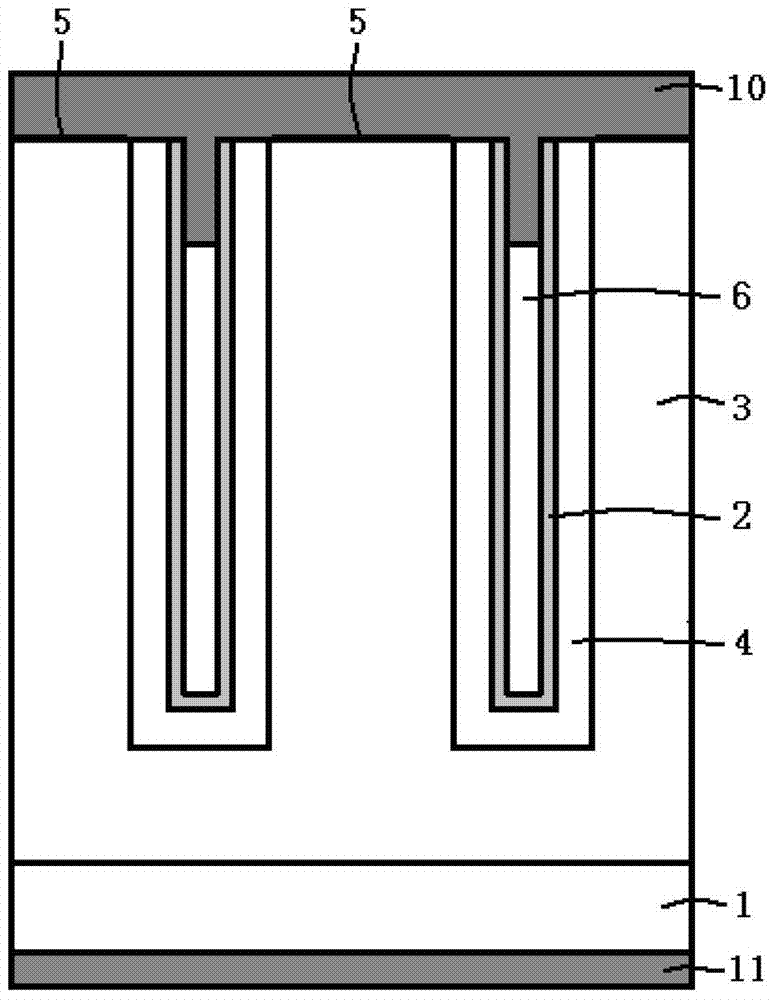
[0024] figure 2 It is a cross-sectional view of a trench structure charge compensation Schottky semiconductor device of the present invention, combined below figure 2 The semiconductor device of the present invention will be described in detail.
[0025] A Schottky semiconductor device, comprising: a substrate layer 1, which is an N conductivity type semiconductor silicon material, and the doping concentration of phosphorus atoms is 1E19 / CM 3 , on the lower surface of the substrate layer 1, the electrodes are drawn out through the lower surface metal layer 11; the first conductive semiconductor material 3, located on the substrate layer 1, is a semiconductor silicon material of N conductivity type, and the doping concentration of phosphorus atoms is 1E16 / CM 3 ; The second conductive semiconductor material 4, located near the inner wall of the trench, is a semiconductor silicon material of P conductivity type, and the doping concentration of boron atoms is 1E16 / CM 3 ; The p...
Embodiment 3
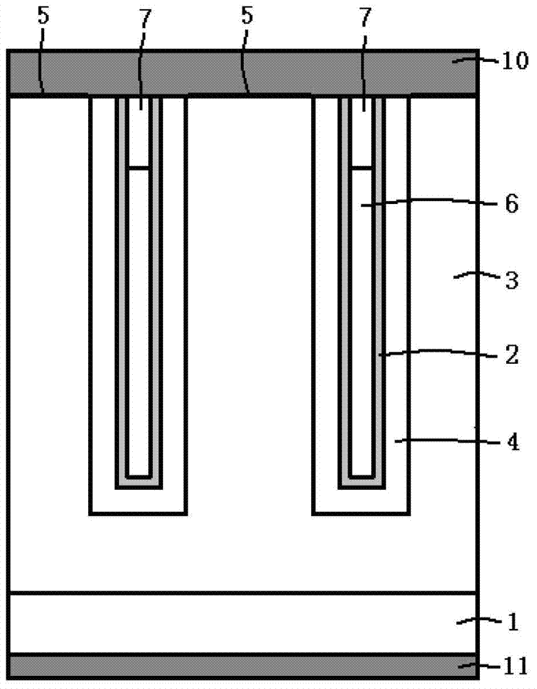
[0034] image 3 It is a cross-sectional view of a trench structure charge compensation Schottky semiconductor device of the present invention, combined below image 3 The semiconductor device of the present invention will be described in detail.
[0035] A Schottky semiconductor device, comprising: a substrate layer 1, which is an N conductivity type semiconductor silicon material, and the doping concentration of phosphorus atoms is 1E19 / CM 3 , on the lower surface of the substrate layer 1, the electrodes are drawn out through the lower surface metal layer 11; the first conductive semiconductor material 3, located on the substrate layer 1, is a semiconductor silicon material of N conductivity type, and the doping concentration of phosphorus atoms is 1E16 / CM 3 ; The second conductive semiconductor material 4, located near the inner wall of the trench, is a semiconductor silicon material of P conductivity type, and the doping concentration of boron atoms is 1E16 / CM 3 ; The pol...
PUM
 Abstract
Description
Claims
Application Information
 - R&D
- Intellectual Property
- Life Sciences
- Materials
- Tech Scout
- Unparalleled Data Quality
- Higher Quality Content
- 60% Fewer Hallucinations
Browse by: Latest US Patents, China's latest patents, Technical Efficacy Thesaurus, Application Domain, Technology Topic, Popular Technical Reports.
© 2025 PatSnap. All rights reserved.Legal|Privacy policy|Modern Slavery Act Transparency Statement|Sitemap|About US| Contact US: help@patsnap.com