Non-volatile semiconductor memory device and readout method thereof
A non-volatile, semiconductor technology, applied in information storage, static memory, read-only memory, etc., can solve the problem of prolonged sensing time, and achieve the effect of avoiding channel boost and shortening sensing time
- Summary
- Abstract
- Description
- Claims
- Application Information
AI Technical Summary
Problems solved by technology
Method used
Image
Examples
Embodiment 1
[0079] Figure 6A is an operation timing chart of the read method of the NAND-type flash EEPROM according to Embodiment 1 of the present invention. exist Figure 6A In 23a, the initial pulse voltages of the select gate lines SGD and SGS start with a voltage rising to a high level. Thereafter, the select gate transistor connected to the select gate line SGD is turned off. Then, the selection gate transistor connected to the selection gate line SGD is turned on and the selection gate transistor connected to the selection gate line SGS is turned off. Then, the selection gate transistor connected to the selection gate line SGD is turned off and the selection gate transistor connected to the selection gate line SGS is turned on.
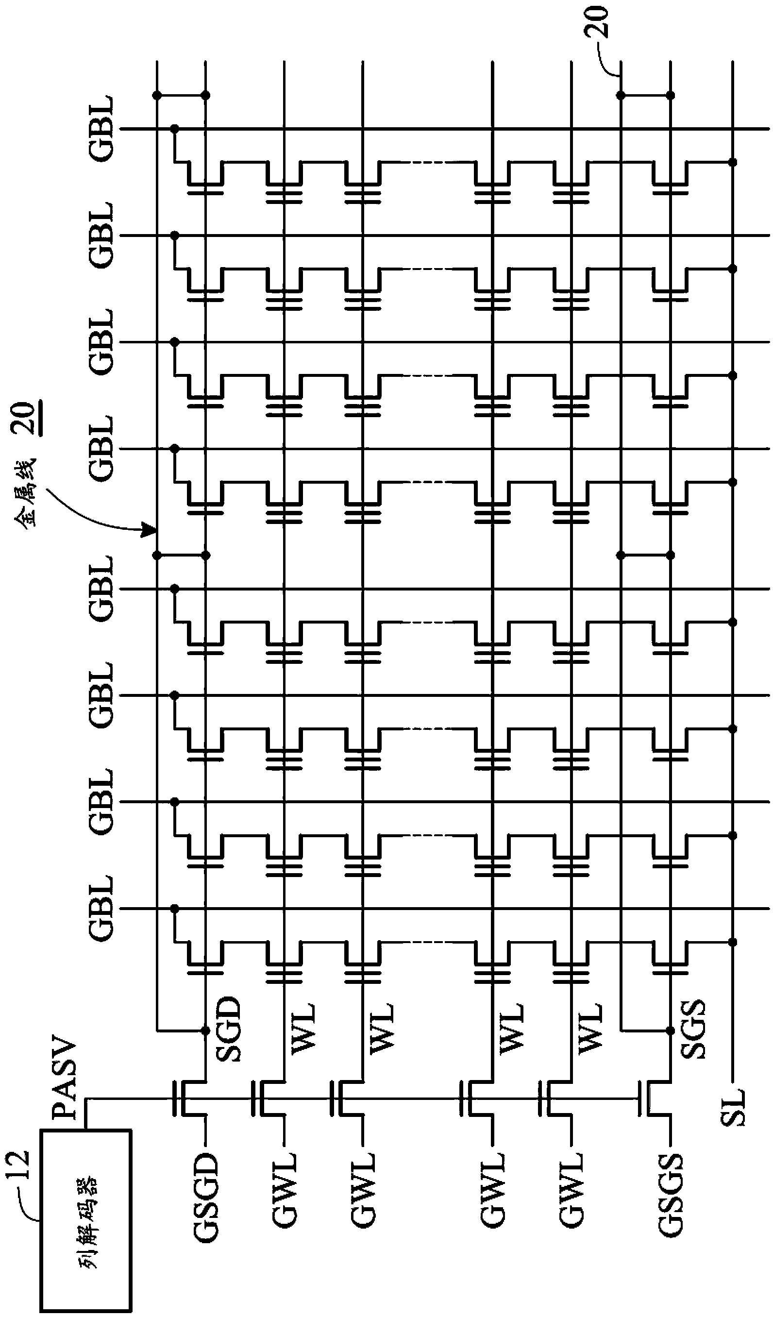
[0080] Here, when the voltage of the word line starts to rise, the voltage rises quickly. For example, if the word line voltage takes 5 µs to reach Figure 4 95% of PASV, which means the voltage has risen to 63% at the time point of 1.7 microseconds....
Embodiment 2
[0082] Figure 6B is an operation timing chart of the read method of the NAND flash EEPROM according to the second embodiment of the present invention. exist Figure 6B In 23b, the initial pulse voltages of the select gate lines SGD and SGS start with a voltage rising to a high level. Thereafter, the select gate transistor connected to the select gate line SGS is turned off. Then, the selection gate transistor connected to the selection gate line SGD is turned off and the selection gate transistor connected to the selection gate line SGS is turned on. Then, the selection gate transistor connected to the selection gate line SGD is turned on and the selection gate transistor connected to the selection gate line SGS is turned off.
Embodiment 3
[0084] Figure 6C It is an operation timing chart of the reading method of the NAND flash EEPROM according to the third embodiment of the present invention. exist Figure 6C In 23c, the initial pulse voltages of the select gate lines SGD and SGS start with a voltage rising to a high level. Thereafter, the select gate transistor connected to the select gate line SGD is turned off. Then, the selection gate transistor connected to the selection gate line SGD is turned on and the selection gate transistor connected to the selection gate line SGS is turned off. Then, the selection gate transistor connected to the selection gate line SGD is turned off and the selection gate transistor connected to the selection gate line SGS is turned on. Furthermore, the above actions are performed repeatedly. In Embodiment 3, the width of the control pulse for turning on / off the selection gate transistor is smaller than that in Embodiments 1 and 2. Meanwhile, in Embodiment 3, the number of co...
PUM
 Abstract
Description
Claims
Application Information
 - R&D
- Intellectual Property
- Life Sciences
- Materials
- Tech Scout
- Unparalleled Data Quality
- Higher Quality Content
- 60% Fewer Hallucinations
Browse by: Latest US Patents, China's latest patents, Technical Efficacy Thesaurus, Application Domain, Technology Topic, Popular Technical Reports.
© 2025 PatSnap. All rights reserved.Legal|Privacy policy|Modern Slavery Act Transparency Statement|Sitemap|About US| Contact US: help@patsnap.com


