Optical/crystal comprehensive film thickness monitoring method
A technology of crystal control and film thickness, which is applied in metal material coating process, vacuum evaporation plating, coating, etc., can solve the problem of large error and reduce the effect of influence
- Summary
- Abstract
- Description
- Claims
- Application Information
AI Technical Summary
Problems solved by technology
Method used
Image
Examples
Embodiment Construction
[0036] The present invention will be further described in conjunction with embodiment and accompanying drawing below.
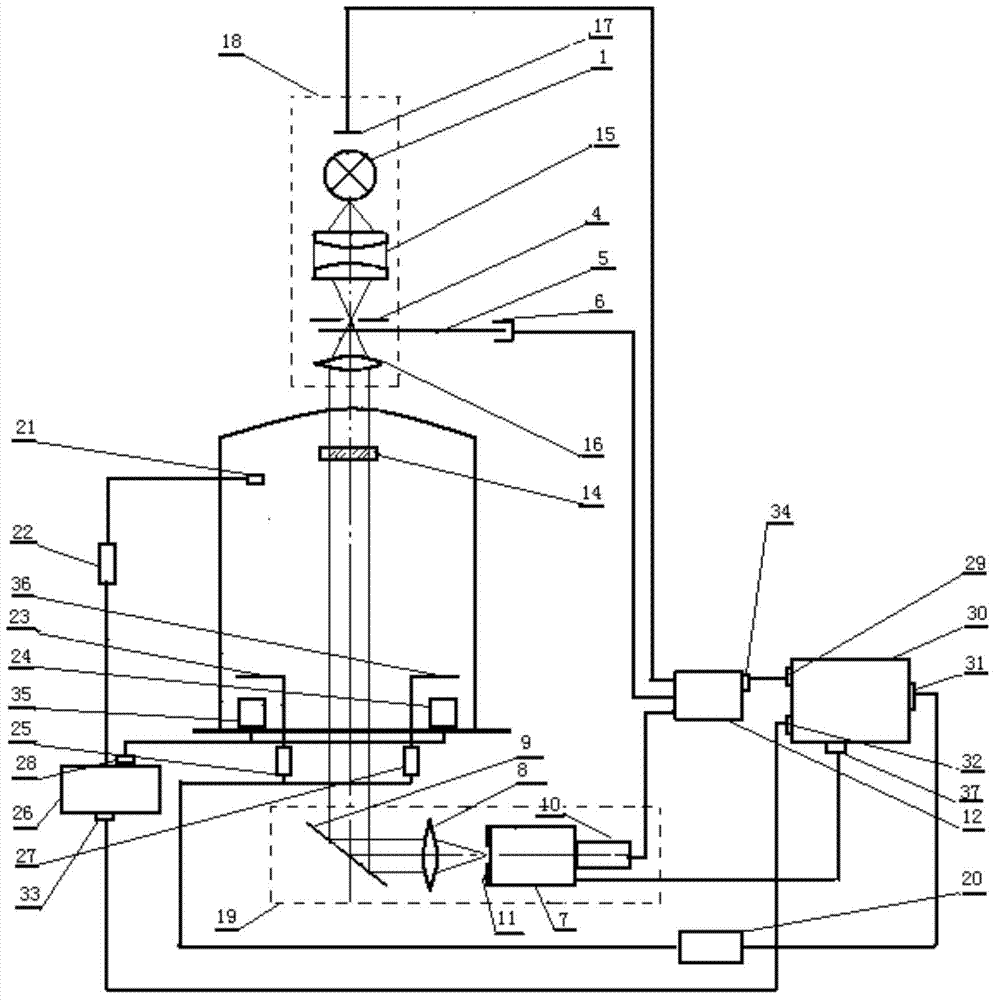
[0037] see first figure 2 , figure 2 It is a schematic structural diagram of the coating device of the film thickness monitoring method for improving optical performance of the present invention. As can be seen from the figure, the coating device used in the present invention comprises a light control-crystal control comprehensive film thickness monitoring system composed of a light source emission system 18, a monitoring sheet system 14, a signal receiving system 19, a lock-in amplifier 12 and a crystal controller 26. system, and a computer 30 with a control program, a damper switch control circuit 20. Lock-in amplifier 12, crystal control instrument 26, monochromator 7 are connected with the first serial port 29, the second serial port 32, the third serial port 37 of the computer 30 with the RS232 serial port of carrying and control program respectively...
PUM
 Abstract
Description
Claims
Application Information
 - R&D
- Intellectual Property
- Life Sciences
- Materials
- Tech Scout
- Unparalleled Data Quality
- Higher Quality Content
- 60% Fewer Hallucinations
Browse by: Latest US Patents, China's latest patents, Technical Efficacy Thesaurus, Application Domain, Technology Topic, Popular Technical Reports.
© 2025 PatSnap. All rights reserved.Legal|Privacy policy|Modern Slavery Act Transparency Statement|Sitemap|About US| Contact US: help@patsnap.com


