PCB and method for embedding driven elements in PCB

A technology of passive components and PCB boards, applied in the direction of printed circuits connected with non-printed electrical components, assembled printed circuits with electrical components, etc., can solve the problem of not being able to set more components, and achieve easy BOM management and BOM realization management, low noise effect

Active Publication Date: 2014-01-01
恒科科技产业有限公司
View PDF3 Cites 3 Cited by
  • Summary
  • Abstract
  • Description
  • Claims
  • Application Information

AI Technical Summary

Problems solved by technology

[0004] In view of the deficiencies in the prior art above, the purpose of the present invention is to provide a PCB board and a method for embedding passive components in the PCB board, aiming to solve the problem that the current PCB cannot be equipped with more components

Method used


Image

  • PCB and method for embedding driven elements in PCB
  • PCB and method for embedding driven elements in PCB
  • PCB and method for embedding driven elements in PCB

Examples


Embodiment Construction

[0028] The present invention provides a PCB board and a method for embedding passive components in the PCB board. In order to make the purpose, technical solution and effect of the present invention clearer and clearer, the present invention will be further described in detail below. It should be understood that the specific embodiments described here are only used to explain the present invention, not to limit the present invention.

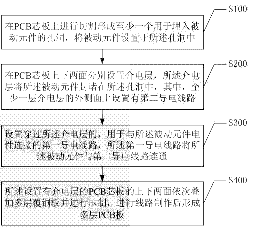
[0029] Such as figure 1 A method for embedding passive components in a PCB board is shown, wherein the method includes the following steps:

[0030] S100, cutting on the PCB core board to form at least one hole for embedding passive components, and disposing the passive components in the hole.

[0031] The passive components include components such as capacitors, resistors, inductors, and magnetic beads. The holes are formed by laser drilling or a blind routing process (Depth control routing). Preferably, the holes of the present invention are ...


PUM


Abstract

The invention discloses a PCB and a method for embedding driven elements in the PCB. The method comprises the steps that A holes are formed in a PCB core plate through cutting, and then the driven elements are placed in the holes; B the upper face and the lower face of the PCB core plate are respectively provided with a dielectric layer, and the dielectric layers seal the driven elements in the holes, wherein a second conductive circuit is arranged on the outer side face of at least one dielectric layer; C a first conductive circuit which penetrates through the dielectric layers and is used for being electrically connected with the driven elements is arranged, and the first conductive circuit enables the driven elements and the second conductive circuit to be communicated. According to the PCB and the method, traditional surface-mounted driven elements are embedded in the PCB, space of the PCB is saved, more components can be arranged on the PCB which can have more functions, and compared with surface-mounted elements, the embedded driven elements are shorter in transmission path of signals and smaller in noise, and BOM management can be realized more easily.

Description

technical field [0001] The invention relates to PCB board packaging technology, in particular to a PCB board and a method for embedding passive components in the PCB board. Background technique [0002] With the widespread application of smart products such as mobile phones, the competition among smart product manufacturers is becoming more and more fierce, and each manufacturer will launch several products with different highlights every year. Taking a mobile phone as an example, on the premise that the size of the mobile phone is similar, the more functions are designed, the more highlights will attract customers. However, due to the limitations of the motherboard, device distance and PCB size, it is very difficult to add more components to further add new functions. [0003] Therefore, the prior art still needs to be improved and developed. Contents of the invention [0004] In view of the above-mentioned deficiencies in the prior art, the purpose of the present inven...

Claims


Application Information

Patent Timeline
IPC IPC(8): H05K3/32H05K1/18
Inventor 王佳
Owner 恒科科技产业有限公司
Why Eureka
Try Eureka