
Magnetic element and method of programming magnetic memory

A technology of magnetic components and devices, applied in the field of programming magnetic memory, can solve the problems of dead magnetic area enhancement, disordered interface, attenuation, etc.

Active Publication Date: 2018-02-09
SAMSUNG ELECTRONICS CO LTD
View PDF4 Cites 0 Cited by
  • Summary
  • Abstract
  • Description
  • Claims
  • Application Information

AI Technical Summary

Problems solved by technology

The direct exposure of the conventional free layer 20 to the top contact 24 may lead to disordered interfaces, dead magnetic regions and enhanced decay

Method used


Image

  • Magnetic element and method of programming magnetic memory
  • Magnetic element and method of programming magnetic memory
  • Magnetic element and method of programming magnetic memory

Examples


Embodiment Construction

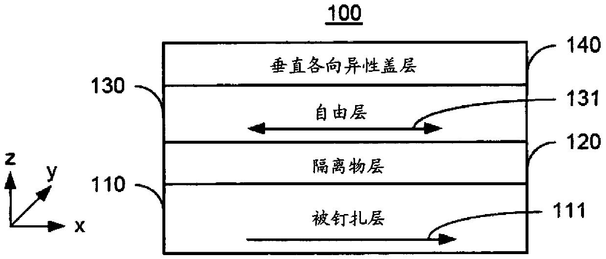
[0028] Exemplary embodiments relate to magnetic elements that may be used in magnetic devices such as magnetic memories, and devices using such magnetic elements. The following description is given to enable one of ordinary skill in the art to make and use the invention, and is provided in the context of a patent application and its claims. Various modifications to the exemplary embodiments and the general principles and features described herein will be readily apparent. The exemplary embodiments are described primarily in terms of particular methods and systems provided in particular implementations. However, these methods and systems will work effectively in other implementations. Phrases such as "exemplary embodiment," "one embodiment," and "another embodiment" can refer to the same or different embodiments as well as multiple embodiments. Embodiments will be described with respect to systems and / or devices having particular components. However, the systems and / or devic...


PUM


Abstract

In one embodiment, a magnetic element for a semiconductor device includes a reference layer, a free layer, and a non-magnetic spacer layer disposed between the reference layer and the free layer. The non-magnetic spacer layer includes binary, ternary or multi-alloy oxide materials. Binary, ternary or multi-component alloy oxide materials include MgO with one or more additional elements selected from the group consisting of: Ru, Al, Ta, Tb, Cu, V, Hf, Zr, W, Ag, Au, Fe, Co, Ni, Nb, Cr, Mo and Rh.

Description

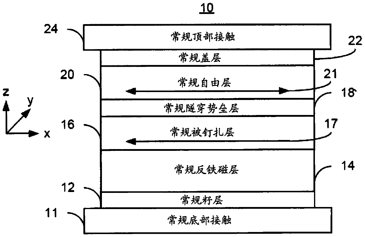
technical field [0001] The inventive concept relates to a magnetic element for a semiconductor device and a method of programming a magnetic memory. Background technique [0002] Magnetic memory, especially Magnetic Random Access Memory (MRAM), has attracted increasing attention due to its potential for high read / write speed during operation, excellent endurance, non-volatility, and low power consumption. focus on. MRAM can store information using magnetic materials as an information recording medium. One type of MRAM is spin-transfer torque random-access memory (STT-RAM). STT-RAM utilizes a magnetic element, at least in part, to write to the magnetic element with an electric current driven through the magnetic element. [0003] For example, figure 1 An exemplary magnetic tunnel junction (MTJ) 10 is depicted, which can be used in conventional STT-RAM. A conventional MTJ 10 is typically formed on a bottom contact 11 using a conventional seed layer(s) 12 and including a p...

Claims


Application Information

Patent Timeline
Patent Type & Authority Patents(China)
IPC IPC(8): H01L43/08H01L43/10G11B5/66
CPCG11C11/1659G11C11/161G11C11/16H01L21/02362H10B61/00H10N50/01H10N50/10
Inventor 陈友君唐学体
Owner SAMSUNG ELECTRONICS CO LTD
Learn More