Array substrate, preparing method of array substrate and display device of array substrate

An array substrate and substrate technology, applied in the field of array substrates and their preparation methods, and display devices, can solve problems such as light leakage, poor orientation of liquid crystal molecules, and easy light leakage of data lines, etc., so as to improve light transmittance, increase contrast, and ensure quality Effect

Active Publication Date: 2014-01-01
HEFEI BOE OPTOELECTRONICS TECH +1
View PDF5 Cites 6 Cited by
  • Summary
  • Abstract
  • Description
  • Claims
  • Application Information

AI Technical Summary

Problems solved by technology

Usually, the orientation of the liquid crystal molecules in the weak friction area is poor. In the black state or white state, the liquid crystal molecules in the weak friction area may not be oriented in a specific direction, resulting in light leakage; when the array substrate and the color filter substrate are combined Finally, when the black matrix cannot cover the friction weak area, the light leakage will show up
[0006] Usually, the width of the black matrix in the corresponding color filter substrate above the gate line is relatively large, so light leakage rarely occurs near the gate line; and in order not to affect the aperture ratio of the display panel, the width of the corresponding black matrix above the data line is generally small , in the case of poor alignment between the array substrate and the color filter substrate, light leakage is often prone to occur near the data lines, especially in the areas corresponding to the edges of the data lines

Method used


Image

  • Array substrate, preparing method of array substrate and display device of array substrate
  • Array substrate, preparing method of array substrate and display device of array substrate
  • Array substrate, preparing method of array substrate and display device of array substrate

Examples


Embodiment 1

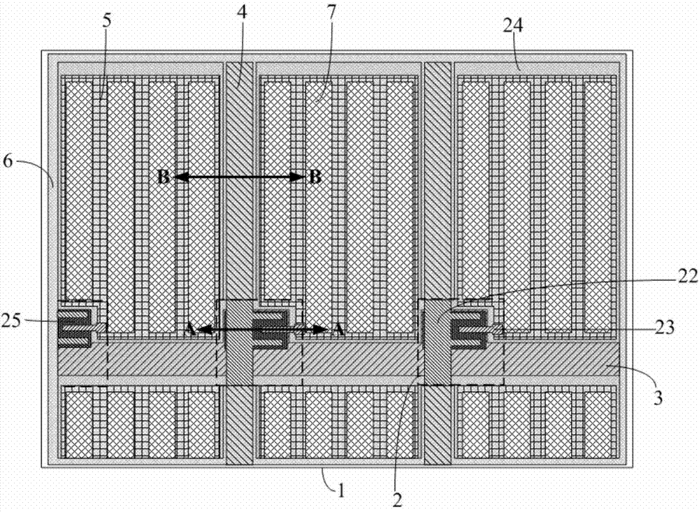
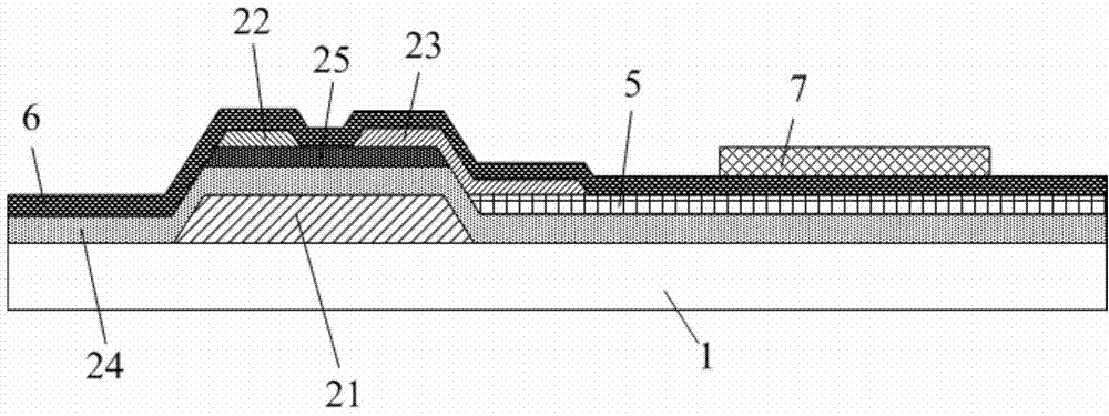
[0036] This embodiment provides an array substrate, such as figure 1 and figure 2 As shown, it includes: a substrate 1 and a thin film transistor 2 arranged on the substrate 1, a gate line 3 and a data line 4. The thin film transistor 2 includes a gate 21, a source 22 and a drain 23 arranged on the same layer, and a gate line 2 arranged on the gate. The gate insulating layer 24 between the electrode 21 and the source electrode 22 and the drain electrode 23, the gate electrode 21 is electrically connected to the gate line 3, the data line embedded area is arranged in the gate insulating layer 24, and the data line 4 is arranged in the data line embedded area , the data line 4 is electrically connected to the source 22 .

[0037] In addition, in this embodiment, the thin film transistor further includes an active layer 25 disposed between the source 22 and the drain 23 and the gate insulating layer 24 and corresponding to the gate 21 .

[0038] Wherein, the gate line 3 and th...

Embodiment 2

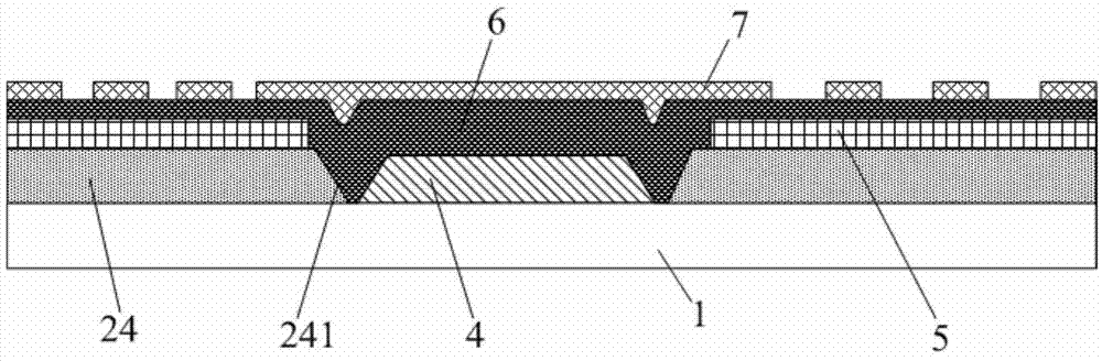
[0067] This embodiment provides an array substrate, and the difference from Embodiment 1 is that, as Figure 5 As shown, the strip-shaped groove 241 is opened on the surface layer of the gate insulating layer 24, and the depth of the strip-shaped groove 241 is smaller than the thickness of the gate insulating layer 24, the data line 4 is arranged at the bottom of the strip-shaped groove 241, and the height of the data line 4 is less than or equal to The depth of the strip groove 241. Such an arrangement also enables the data lines 4 to be completely embedded in the bar-shaped grooves 241 , so that the data lines 4 form only a small or no gap with respect to other regions in the pixel region.

[0068] Also, since the gridlines ( Figure 5 (not shown in ) is arranged under the gate insulating layer 24, so there is a thin layer of gate insulating layer 24 between the data line 4 and the gate 21 / gate line 3, and the thin layer of gate insulating layer 24 The thickness is the dif...

Embodiment 3

[0080] This embodiment provides an array substrate. The difference from Embodiment 1-2 is that the positions of the common electrode and the pixel electrode in the array substrate are interchanged, that is, the pixel electrode is arranged above the passivation layer, and the pixel electrode is a strip-shaped narrow a slit structure; and the common electrode is arranged between the gate insulating layer and the passivation layer, and the common electrode is plate-shaped.

[0081] Correspondingly, based on the preparation method of the array substrate in Embodiment 1, in the preparation method of the array substrate, the step of forming the pixel electrode (ie, step S4) and the step of forming the common electrode (ie, step S7) can be interchanged. .

[0082]Other structures, sizes, materials and manufacturing methods of the array substrate in this embodiment are the same as those in Embodiment 1 or 2, and will not be repeated here.

[0083] The array substrates in Examples 1-3...


PUM


Abstract

The invention provides an array substrate, a preparing method of the array substrate and a display device of the array substrate. The array substrate comprises a substrate body, a thin film transistor, a grid line and a data line, wherein the thin film transistor, the grid line and the data line are arranged on the substrate body. The thin film transistor comprises a grid electrode, a source electrode, a drain electrode and a grid insulating layer arranged between the grid electrode, the source electrode and the drain electrode, wherein the grid electrode is electrically connected with the grid line, a data line embedding area is arranged in the grid insulating layer, the data line is positioned in the data line embedding area, and the data line is electrically connected with the source electrode. The array substrate is arranged in the data line embedding area of the grid insulating layer through the data line, so that no offset or small offset is generated in the edge area, corresponding to other areas in a pixel area, of the data line. Thus, no friction weak area is generated in alignment layer friction, no light leakage is generated, accordingly the black array width above the data line is reduced, and the aperture opening rate of a display panel is improved. The display device uses the array substrate to improve contract ratio and light transmittance.

Description

technical field [0001] The present invention relates to the field of display technology, in particular, to an array substrate, a manufacturing method thereof, and a display device. Background technique [0002] With the development of display technology, people have higher and higher requirements for display devices with high brightness, high contrast and low energy consumption. [0003] Currently, flat panel display devices are prevalent, and the flat panel display devices generally face the problem of how to avoid light leakage during the manufacturing process. [0004] For example, for an ADS (Advanced Super Dimension Switch, Advanced Super Dimension Switching Technology) mode liquid crystal display device, the display panel is prone to light leakage when it is in a black state, and this light leakage will cause the brightness of the black state of the display panel to be high , resulting in low contrast of the display panel; for liquid crystal display devices in HADS (H...

Claims


Application Information

Patent Timeline
IPC IPC(8): H01L27/12H01L29/786H01L21/77G02F1/1362G02F1/1368
Inventor 赵海廷
Owner HEFEI BOE OPTOELECTRONICS TECH
Why Eureka
Try Eureka