
System and method for modeling printed circuit board level conducted electromagnetic interference

A technology of conducting electromagnetic interference and printed circuit boards, which is applied in the direction of program control devices, electrical digital data processing, software simulation/interpretation/simulation, etc. It can solve problems that affect the research and development cycle and cost, achieve optimal design, and improve system performance. , cost-saving effect

Active Publication Date: 2014-01-01
DONGFANG ELECTRIC CORP LTD
View PDF3 Cites 28 Cited by
  • Summary
  • Abstract
  • Description
  • Claims
  • Application Information

AI Technical Summary

Problems solved by technology

Once an electromagnetic compatibility problem occurs, it is generally necessary to redesign and manufacture the board, which affects the development cycle and cost

Method used


Image

  • System and method for modeling printed circuit board level conducted electromagnetic interference
  • System and method for modeling printed circuit board level conducted electromagnetic interference
  • System and method for modeling printed circuit board level conducted electromagnetic interference

Examples


Embodiment 1

[0045] The present invention is a system for quantitative modeling and analysis of circuit board-level conduction electromagnetic interference. Interference performance is optimized.

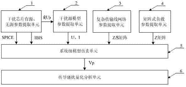
[0046] figure 1 It is a circuit board-level conducted electromagnetic interference modeling system of the present invention. The system includes an interference chip active and passive parameter extraction unit 1, a complex transmission line network parameter extraction unit 2, a matrix load parameter extraction unit 3, and an interference source model parameter extraction unit. Unit 4, system-level model simulation unit 5 and conduction disturbance quantitative analysis unit 6.

[0047] The power module on the circuit board is equivalent to a harmonic voltage source. The main harmonics of the power module are the switching frequency and its higher harmonics. The actual switching frequency of the power module is 300kHz, so it is equivalent to the harmonic source of 300kHz and 600kHz.

[0048...


PUM


Abstract

The invention relates to the field of electromagnetic compatibility, in particular to a system and a method for modeling printed circuit board level conducted electromagnetic interference. Conducted interference of a power wire port of a certain control circuit board is quantitatively analyzed by extraction through a circuit model and modular modeling. Interference noise sources, equivalent resistance R, inductance L, capacitance C, conductance G parameters and internal logic circuits of devices are acquired by respectively calculating and equalizing circuits, main interference chips, power modules and the like on the circuit board, modular package is performed, so that an equivalent circuit model of the whole power system is built, and conducted interference waveforms and quantitative spectra of points on a power wire can be obtained by circuit simulation. Conducted electromagnetic interference frequency and amplitude of key circuits on the printed circuit board can be quantitatively analyzed at a pre-design phase, portions with poor electromagnetic compatibility are found and optimized, the electromagnetic interference degree of the whole circuit board is reduced, and research and development cycle and cost can be reduced.

Description

technical field [0001] The invention relates to the field of electromagnetic compatibility, and specifically refers to a system and method for modeling, analyzing and quantitatively predicting the amplitude and frequency of conducted electromagnetic interference in printed circuit board level electromagnetic compatibility. Background technique [0002] According to the definition in the national standard GB / T4365 Electromagnetic Compatibility (EMC) terminology, electromagnetic compatibility refers to the ability of a device or system to work normally in its electromagnetic environment without causing unacceptable electromagnetic disturbance to anything in the environment. Electromagnetic compatibility includes two aspects of electromagnetic interference (EMI) and electromagnetic susceptibility (EMS). [0003] Electromagnetic interference (EMI) is the degradation of equipment, transmission channels or system performance caused by electromagnetic disturbance. Electromagnetic ...

Claims


Application Information

Patent Timeline
IPC IPC(8): G06F17/50G06F9/455G06F19/00
Inventor 肖文静唐健王多平边晓光
Owner DONGFANG ELECTRIC CORP LTD
Learn More