Pixel circuit and displayer

A pixel circuit and pixel technology, applied in static indicators, instruments, etc., can solve the problems of high performance requirements of TFT devices, reduced pixel spacing, and difficulty, and achieve the goal of reducing size, increasing the number of pixels, and reducing pixel spacing. Effect

Active Publication Date: 2013-12-25
BOE TECH GRP CO LTD +1
View PDF5 Cites 8 Cited by
  • Summary
  • Abstract
  • Description
  • Claims
  • Application Information

AI Technical Summary

Problems solved by technology

However, it is not easy to arrange 6 thin film transistors and 1 capacitor in one pixel, and the TFT device needs to be made very small, so the performance requirements of the TFT device are relatively high, which will lead to pixel pitch (Pixel Pitch) cannot be further reduced

Method used


Image

  • Pixel circuit and displayer
  • Pixel circuit and displayer
  • Pixel circuit and displayer

Examples


Embodiment Construction

[0068] Embodiments of the present invention provide a pixel circuit and a display, which are used to reduce the size of the pixel circuit, further reduce the pixel pitch, increase the number of pixels in a unit area, and improve the image display quality.

[0069] Wherein, the pixel circuit provided in the embodiment of the present invention is an active matrix light emitting diode pixel circuit. Since the active matrix light emitting diode pixel circuit can play a role in compensating the driving module of the pixel, the active matrix light emitting diode pixel circuit in the present invention The circuit may also be referred to as an active matrix LED pixel compensation circuit.

[0070] A detailed introduction to the technical solutions provided by the embodiments of the present invention is given below.

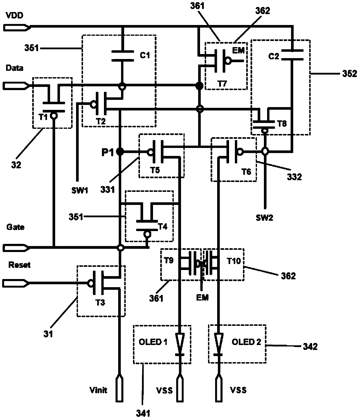
[0071] Such as image 3 As shown, an active matrix light-emitting diode pixel circuit provided by an embodiment of the present invention includes: a first pixel sub-circ...


PUM


Abstract

The invention discloses a pixel circuit and a displayer. According to the pixel circuit, the size of the pixel circuit is reduced, so that the distance between every pixels is reduced, the number of the pixels contained in unit area is increased, and the display quality of an image is improved. The pixel circuit comprises a first pixel sub circuit, a second pixel sub circuit, an initializing module and a data voltage write-in module, wherein the initializing module and the data voltage write-in module are connected with the first pixel sub circuit and the second pixel sub circuit. The initializing module is connected with a reset signal end and a low potential end and used for initializing the first pixel sub circuit and the second pixel sub circuit under the control of a reset signal input by the reset signal end. The data voltage write-in module is connected with data voltage and a gate signal end and used for writing first data voltage in the first pixel sub circuit under the control of a signal input by the gate signal end, compensating a driving module of the first pixel sub circuit, writing second data voltage in the second pixel sub circuit and compensating a driving module of the second pixel sub circuit.

Description

technical field [0001] The invention relates to the technical field of displays, in particular to a pixel circuit and a display. Background technique [0002] At present, the backplane of high-end small and medium-sized active matrix organic light emitting diode (Active Matrix Organic Light Emitting Diode, AMOLED) products mostly uses low temperature polysilicon (Low Temperature Poly-Silicon, LTPS) process technology, but due to the fluctuation of LTPS process, the thin film transistor The threshold voltage of the (Thin Film Transistor, TFT) device drifts, which makes the current driving the Organic Light Emitting Diode (OLED) device unstable, resulting in a decrease in picture display quality. The pixel compensation circuit in the prior art is a 6T1C circuit (a circuit composed of 6 thin film transistors and 1 capacitor), the circuit diagram is as follows figure 1 As shown in the figure, VDD is a high voltage level signal, VSS is a low voltage level signal, Data is a data ...

Claims


Application Information

Patent Timeline
Patent Type & Authority Applications(China)
IPC IPC(8): G09G3/32
CPCG09G3/3233G09G2300/0426G09G2300/0465G09G2300/0814G09G2300/0819G09G3/3258
Inventor 陈俊生
Owner BOE TECH GRP CO LTD
Why Eureka
Try Eureka