Wafer level optical sensor package and low profile camera module, and method of manufacture

A technology for optical sensors and cameras, applied in electric solid state devices, semiconductor devices, radiation control devices, etc., and can solve problems such as light leakage

Active Publication Date: 2013-12-18
STMICROELECTRONICS SRL
View PDF18 Cites 67 Cited by
  • Summary
  • Abstract
  • Description
  • Claims
  • Application Information

AI Technical Summary

Problems solved by technology

However, there exists figure 2 Some issues associated with the configuration shown in , including potential light leaks

Method used


Image

  • Wafer level optical sensor package and low profile camera module, and method of manufacture
  • Wafer level optical sensor package and low profile camera module, and method of manufacture
  • Wafer level optical sensor package and low profile camera module, and method of manufacture

Examples


Embodiment Construction

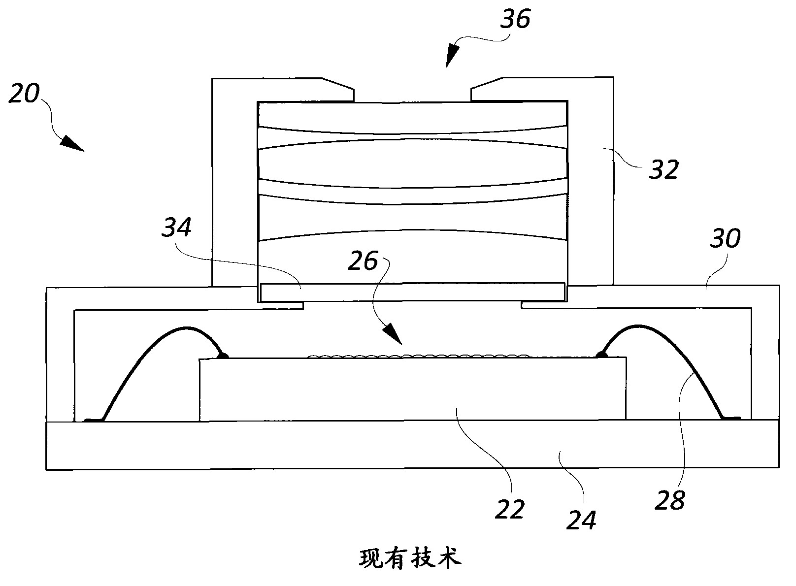
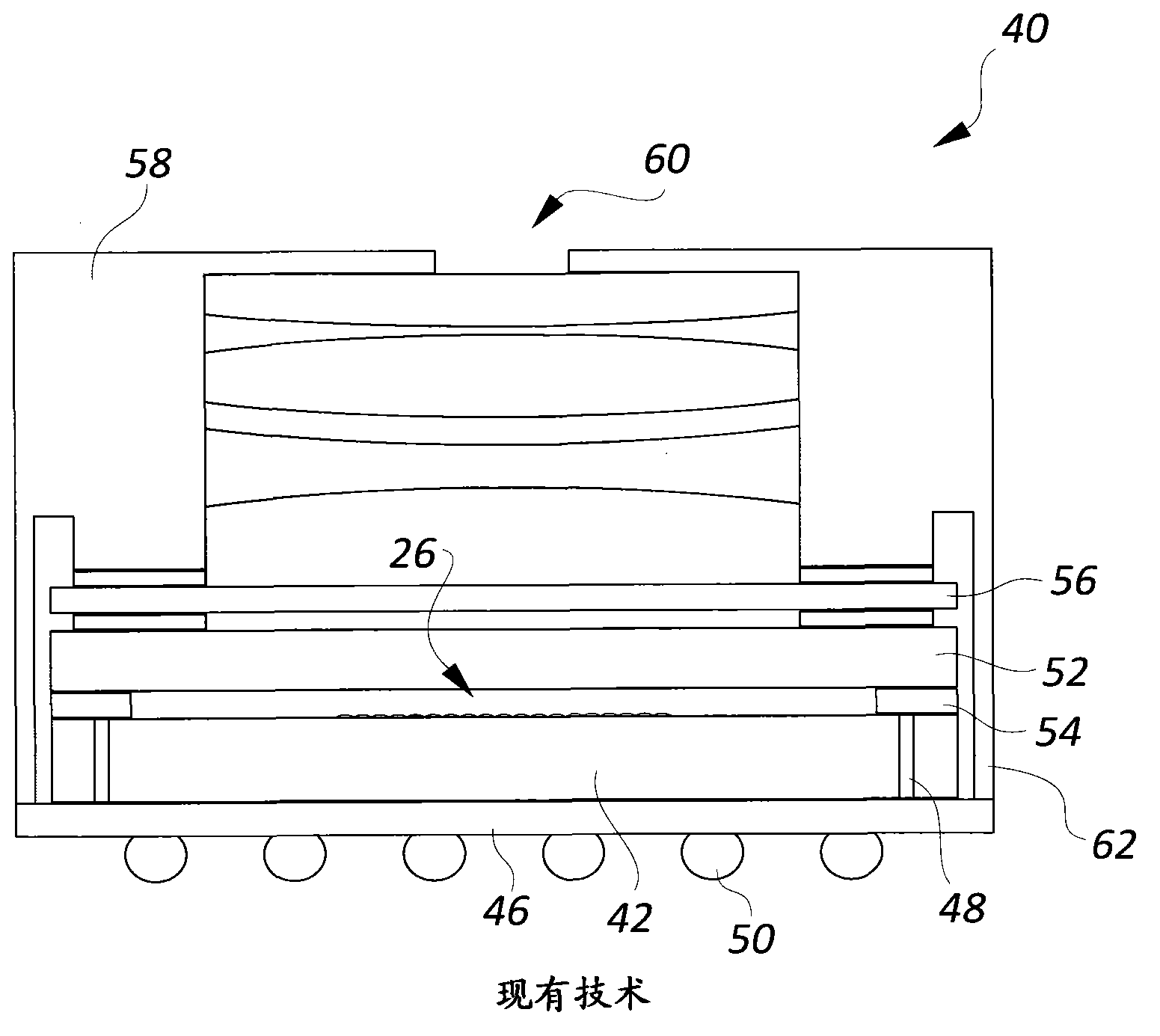
[0022] although figure 2 A prior art example of figure 1 The example of has a reduced height, but the inventors realize that there are a number of problems that may be associated with the second example. First, the associated semiconductor wafer and glass cover must be thinned to their final thickness before the wafer is singulated into individual die. However, if they are too thin, they become extremely brittle and will break during splitting. Furthermore, handling of the glass and die assemblies by assembly workers or robotic machinery used to assemble the camera modules can easily damage them. Also, planarity is an issue because the thinned die can bend slightly during assembly, causing the optical sensor to not function correctly or produce distorted images. Another problem is light leakage. If the lens assembly is not perfectly optically dense, or if any light scattering occurs inside the lens assembly, light can be transmitted from the edge of the cover glass into t...


PUM


Abstract

The invention provides a wafer lever optical sensor package and low profile camera module and a method of manufacture. The wafer-level camera sensor package includes a semiconductor substrate with an optical sensor on a front surface. Through-silicon-vias (TSV) extend through the substrate and provide I / O contact with the sensor from the back side of the substrate. A glass cover is positioned over the front surface, and the cover and substrate are embedded in a molding compound layer (MCL), the front surface of the MCL lying coplanar with the front of the cover, and the back surface lying coplanar with the back of the substrate. Surface-mount devices, electromagnetic shielding, and through-wafer-connectors can be embedded in the MCL. A redistribution layer on the back surface of the MCL includes bottom contact pads for mounting the package, and conductive traces interconnecting the contact pads, TSVs, surface-mount devices, shielding, and through-wafer-connectors. Anisotropic conductive adhesive is positioned on the front of the MCL for physically and electrically attaching a lens array.

Description

technical field [0001] Embodiments of the present invention relate to wafer level packaging for optical sensor devices, particularly packaging in which sensor components are embedded in layers of mold compound, and also to camera modules including such packaging. Background technique [0002] With regard to coupling the optical sensor to the camera circuit, the challenge for the designer is that the device must be positioned on the substrate with the optical sensor facing outward, without any obstructions that might interfere with the reception of the optical image. It is therefore necessary to couple the circuit to the contact pads that do not cover the optical sensor using techniques that are generally not compatible with correct operation of the optical sensor. Furthermore, since camera modules are more commonly used in small electronic devices such as cell phones and tablet computers, there is strong market pressure to reduce the height of the modules so that they can fi...

Claims


Application Information

Patent Timeline
Patent Type & Authority Applications(China)
IPC IPC(8): H01L27/146
CPCH01L27/14618H01L2924/0002H01L27/14625H01L2924/00
Inventor 栾竟恩
Owner STMICROELECTRONICS SRL
Why Eureka
Try Eureka