
PCB limiting and testing fixture

A technology for PCB boards and test fixtures, applied in the field of fixtures, can solve the problems of crushed test points, poor air blowing effect, residual dust and waste chips, etc., to achieve high safety and reliability, good air blowing effect, and improve processing quality. Effect

Inactive Publication Date: 2013-11-27
KUSN MAIZHI FIXTURE TECH
View PDF4 Cites 7 Cited by
  • Summary
  • Abstract
  • Description
  • Claims
  • Application Information

AI Technical Summary

Problems solved by technology

[0003] In order to solve the problem that a lot of dust and waste will remain on the PCB board in the prior art, this will affect the test accuracy of the PCB board. At the same time, the blowing mechanism has a poor blowing effect, and the probe will crush the test point during the pressing process, resulting in For the problem of PCB board damage, the present invention provides a PCB board limit test fixture with simple structure, good blowing effect, improved processing quality, and can limit the probe stroke, making the test safer and more reliable.

Method used


Image

  • PCB limiting and testing fixture

Examples


Embodiment Construction

[0013] The present invention will be further described below in conjunction with the accompanying drawings.

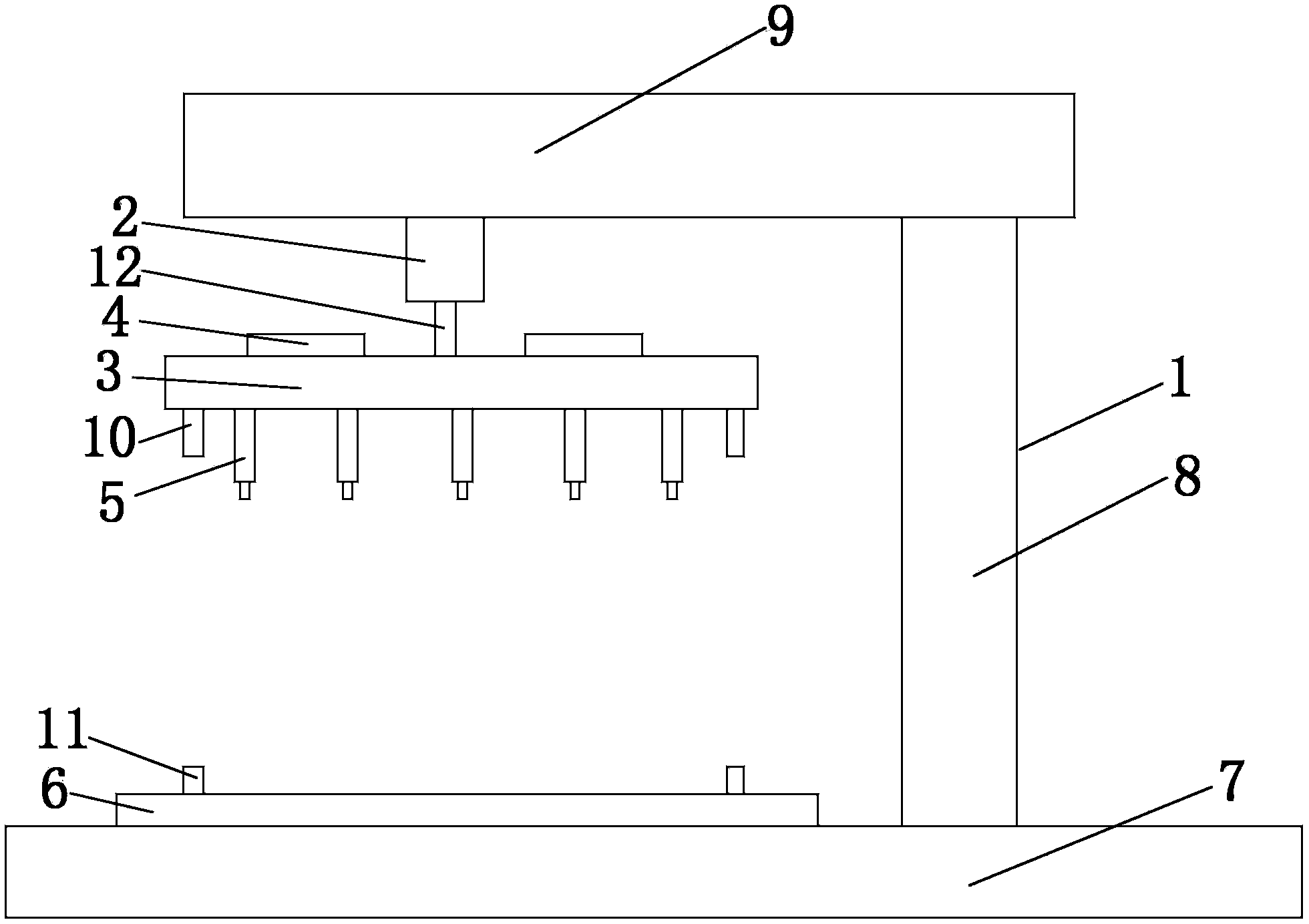
[0014] like figure 1 As shown, a PCB board limit test fixture includes a bracket 1, a cylinder 2, a moving plate 3, a blower 4, a probe 5 and a carrier plate 6, and the bracket 1 includes a base 7, a support beam 8 and a top plate 9, A supporting beam 8 is arranged on the top of the base 7, a top plate 9 is arranged on the top of the supporting beam 8, a carrier plate 6 is arranged on the top of the base 7, and a cylinder 2 is arranged on the bottom of the top plate 9, the cylinder rod 12 of the cylinder 2 and the moving plate 3 connection, the moving plate 3 is provided with several rows of through blowing holes, two blowers 4 are arranged on the top of the moving plate 3, and several probes 5 are connected to the bottom of the moving plate 3, and the probes 5 face The PCB board located in the carrier board 6 .

[0015] On the bottom of the moving plate 3 , upper ba...


PUM


Abstract

The invention discloses a PCB limiting and testing fixture. The PCB limiting and testing fixture comprises a support, and is characterized in that a supporting beam is arranged on the top of a base, a top plate is arranged on the top of the supporting beam, a carrier plate is arranged on the top of the base, an air cylinder is arranged at the bottom of the top plate, an air cylinder rod of the air cylinder is connected with a moving plate, the moving plate is provided with a plurality of rows of communicated blowing holes, blowers are arranged on the top of the moving plate, the bottom of the moving plate is connected with a plurality of probes, the probes face towards a PCB in the carrier plate, upper baffles are arranged at the bottom of the moving plate, and lower baffles are correspondingly arranged on the top of the carrier plate. By means of the PCB limiting and testing fixture, the problems that PCB testing precision is affected because a large quantity of dust and scraps remain on the PCB, a blowing mechanism is poor in blowing effect and the probes can press testing points to damage in the process of pressing are solved; the PCB limiting and testing fixture is simple in structure, good in blowing effect, and capable of improving machining quality and limiting the stoke of the probes.

Description

technical field [0001] The invention relates to a fixture, in particular to a PCB board limit test fixture. Background technique [0002] The Chinese name of PCB board is printed circuit board, also known as printed circuit board and printed circuit board. It is an important electronic component, a support for electronic components, and a provider of electrical connections for electronic components. Because it is made using electronic printing, it is called a "printed" circuit board. At present, during the process of PCB board processing, a lot of dust and waste will remain on the PCB board, which will affect the test accuracy of the PCB board. In addition, the current blower equipment is generally set on the outside of the PCB board, blowing air from the outside to the PCB board. The dust and waste in the middle of the PCB cannot be effectively disposed of, and the use effect is poor. In addition, during the current testing process of the PCB board, since there is no stru...

Claims


Application Information

Patent Timeline
Patent Type & Authority Applications(China)
IPC IPC(8): G01R31/28
Inventor 黄锦章潘萍
Owner KUSN MAIZHI FIXTURE TECH
Learn More