Selective absorbing film set of radiation absorbing layer based on mixture
A technology of radiation absorption and mixture, which is applied in the direction of coating, layered products, sputtering coating, etc., can solve the problems of very strict equipment sealing requirements, difficult control of process parameters, pollution of the environment, etc., and achieve high photothermal conversion efficiency, The effect of improving industrial production efficiency, good high absorption and low radiation effect
- Summary
- Abstract
- Description
- Claims
- Application Information
AI Technical Summary
Problems solved by technology
Method used
Image
Examples
Embodiment 1
[0033] Cu substrate / TiSiN / Si 3 N 4 / SiO 2 Absorbent film system.
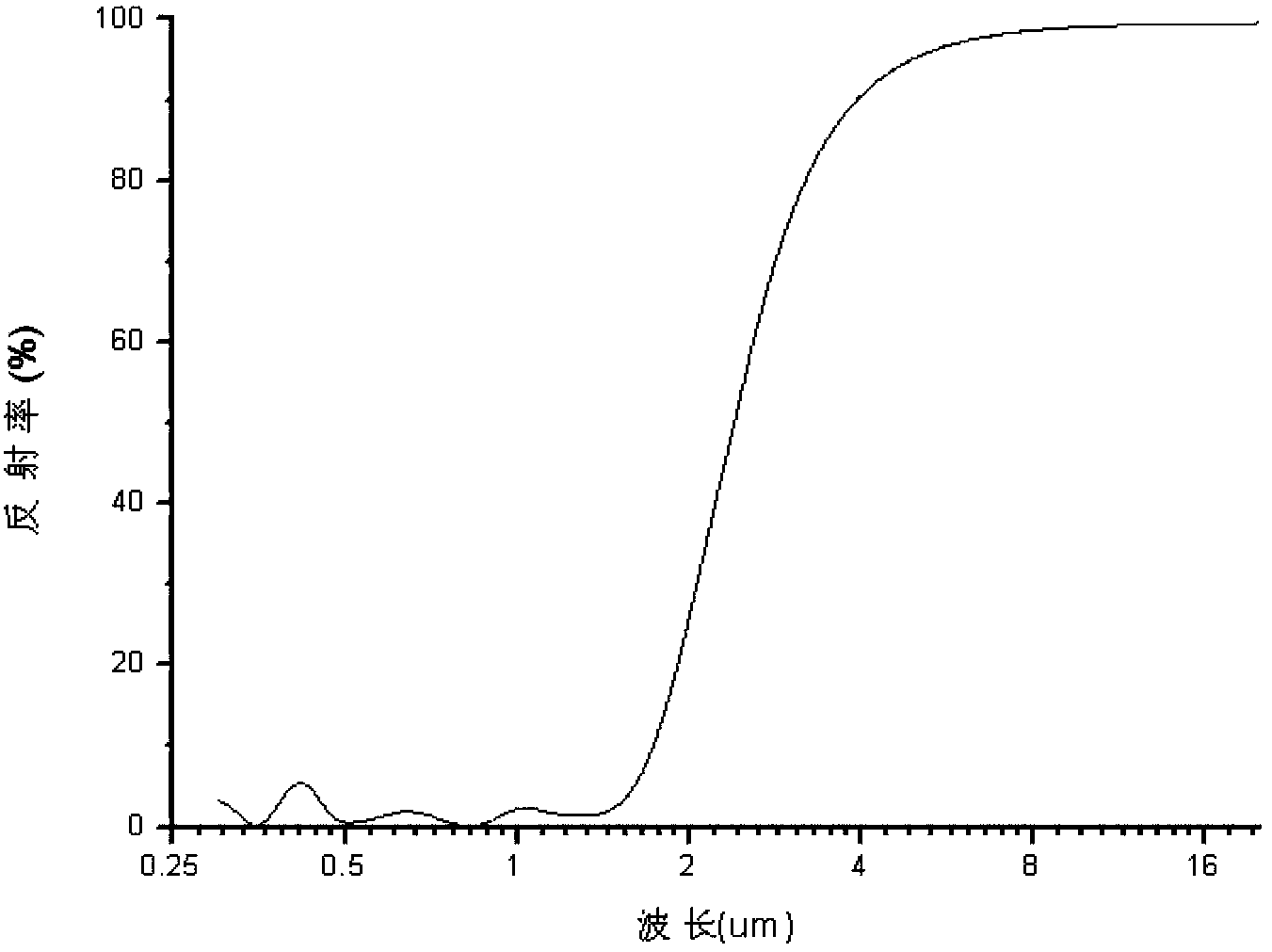
[0034] The absorption film system is specifically: Cu substrate / TiN and Si3N4 mixture film (90nm), the mixing ratio is 0.36:0.64 / Si 3 N 4 Thin film (30nm) / SiO 2 Thin film (65nm).
[0035] The reflection spectrum of the film system is attached figure 2 As shown, the technical indicators of the film system are as follows:
[0036] According to the national standard GB / T6424-2007 and GB / T4271-2007, the absorption rate of this film system reaches 96.5%, and the emissivity is 3.5%.
Embodiment 2
[0038] Cu substrate / NiZnO / ZnO / SiO 2 Absorbent film system.
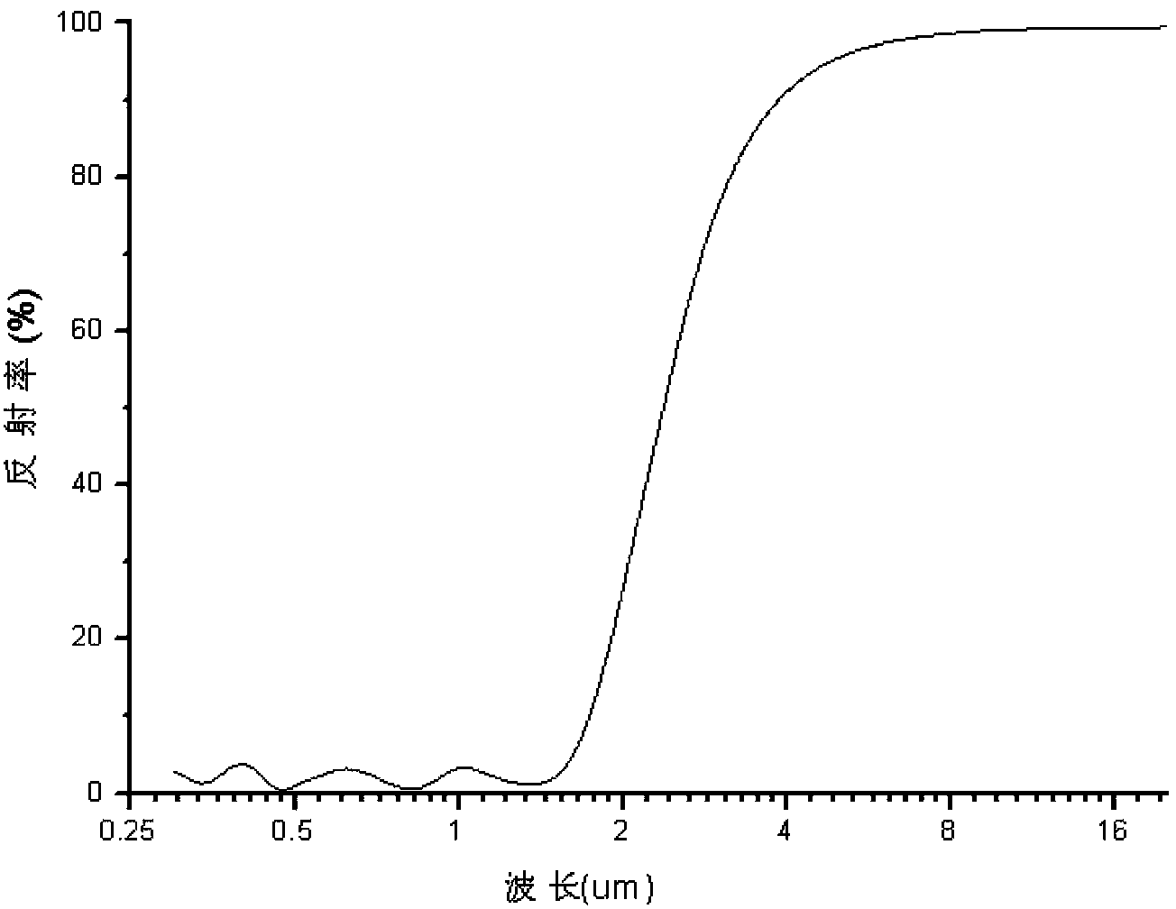
[0039] This absorption film system is specifically: Cu substrate / NiOx and ZnO mixture film (93nm), the mixing ratio is 0.37:0.63 / ZnO film (29nm) / SiO 2 Thin film (70nm).
[0040] The reflection spectrum of the film system is attached image 3 As shown, the technical indicators of the film system are as follows:
[0041] According to the national standard GB / T6424-2007 and GB / T4271-2007, the absorption rate of this film system reaches 97.1%, and the emissivity rate is 2.5%.
Embodiment 3
[0043] Cu substrate / porous TiN / ZnO / SiO 2 / Epoxy resin absorption film system.
[0044] The absorption film system is specifically: Cu substrate / porous TiN mixture film (120nm), the mixing ratio of TiN and pores is 0.75:0.25 / ZnO film (23nm) / SiO 2 Thin film (25nm) / epoxy resin film (26nm).
[0045] The reflection spectrum of the film system is attached Figure 4 As shown, the technical indicators of the film system are as follows:
[0046] According to the national standard GB / T6424-2007 and GB / T4271-2007, the absorption rate of this film system reaches 96.0%, and the emissivity is 4.0%.
PUM
| Property | Measurement | Unit |
|---|---|---|
| thickness | aaaaa | aaaaa |
| thickness | aaaaa | aaaaa |
| thickness | aaaaa | aaaaa |
Abstract
Description
Claims
Application Information
 - R&D
- Intellectual Property
- Life Sciences
- Materials
- Tech Scout
- Unparalleled Data Quality
- Higher Quality Content
- 60% Fewer Hallucinations
Browse by: Latest US Patents, China's latest patents, Technical Efficacy Thesaurus, Application Domain, Technology Topic, Popular Technical Reports.
© 2025 PatSnap. All rights reserved.Legal|Privacy policy|Modern Slavery Act Transparency Statement|Sitemap|About US| Contact US: help@patsnap.com


