Connection structure

A bonding structure and bonding pad technology, applied in the direction of connection, fixed connection, conductive adhesive connection, etc., can solve the problems of short circuit, short circuit of bonding pad, easy to be squeezed to the surrounding area, etc., to reduce accumulation, improve process, avoid The effect of the short circuit phenomenon

Inactive Publication Date: 2013-10-23
TPK TOUCH SOLUTIONS (XIAMEN) INC
View PDF4 Cites 14 Cited by
  • Summary
  • Abstract
  • Description
  • Claims
  • Application Information

AI Technical Summary

Problems solved by technology

A short circuit is easy to occur when using ACF bonding, because the distance between the left and right adjacent bonding pads is small; when pressing, due to the effect of pressure, multiple conductive particles are easily squeezed to the surrounding area 18 , causing the left and right adjacent bonding pads to short-circuit
For example, after lamination, the conductive particles 20 in the ACF layer 14 may be extruded or overflowed (which can be generally referred to as moving) to gather in the peripheral region 18 and be located between two adjacent bonding pads 4 and / or between two adjacent bonding pads 4. between two adjacent bonding pads 10, it is easy to cause a short circuit

Method used


Image

  • Connection structure
  • Connection structure
  • Connection structure

Examples


Embodiment Construction

[0028] The present invention will be further described in detail below in conjunction with the accompanying drawings and specific embodiments.

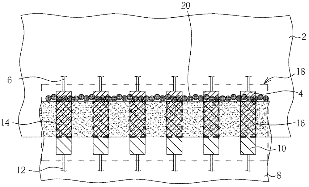
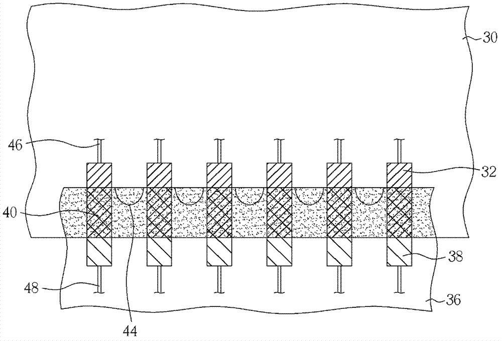
[0029] Figure 2 to Figure 9 It is several specific embodiments according to the present invention. For the convenience of reading, except for Figures 5 and 8, each figure is drawn in a manner that each component is assumed to be transparent, but those skilled in the art should know the relative positions of each component after understanding the present invention. And it should be noted that each element is not drawn according to the actual size ratio.

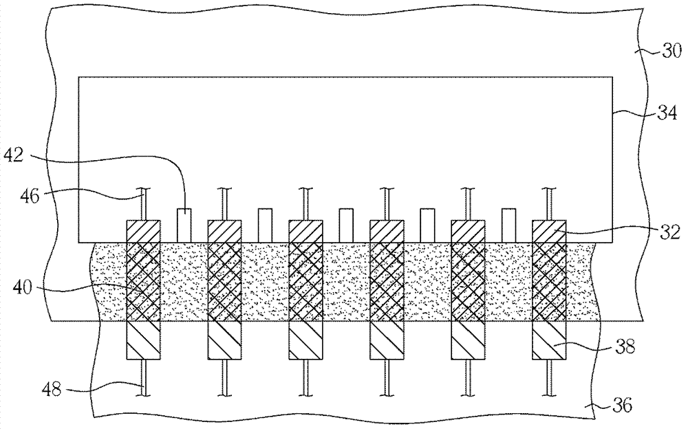
[0030] figure 2 It is a schematic plan view of a bonding structure according to the first embodiment of the present invention. In this bonding structure, a plurality of first bonding pads 32 are located on a first substrate 30 , and the protective layer 34 partially covers each of the first bonding pads 32 . The second substrate 36 and the first substrate 30 are arranged to face...


PUM


Abstract

The invention provides a connection structure including a first substrate, a plurality of first connection gaskets, a second substrate, a plurality of second connection gaskets, anisotropic conductive films (ACFs) and at least one groove structure. The plurality of first connection gaskets are arranged on the first substrate. The second substrate is arranged to be facing part of the first substrate; one face of each of the plurality of second gaskets is arranged on the second substrate and the other face of each of the plurality of second gaskets overlaps part of a corresponding first connection gasket so that first connection areas and peripheral areas which are at peripheries of the connection areas are formed. An ACF are arranged between each first connection gasket and each second connection gasket. The ACFs are provided with a plurality of conductive particles and at least one groove structure is arranged at each of the peripheral areas. When the conductive particles move under a press, the groove structures are capable of accommodating the conductive particles which are moved to the groove structures. In such a way short-circuit phenomena, which are resulted from lamination of the conductive particles, are reduced in connection.

Description

technical field [0001] The invention relates to a bonding structure, in particular to a bonding structure using anisotropic conductive adhesive. Background technique [0002] In the ever-changing information age, electronic products are closely related to people's life and work. With the thinning, miniaturization, precision, and portability of electronic products, in some occasions that cannot be soldered by high-temperature lead-tin, such as: flexible circuit board (FPC), integrated circuit (IC), liquid crystal display ( LCD), touch screen (Touch Panel) and other products of line or pin connection, anisotropic conductive film (hereinafter referred to as ACF) and related line connection methods have been gradually developed to solve Solved various line connection problems of electronic products. [0003] The term ACF referred to herein is intended to include anisotropic conductive films in the form of film layers and anisotropic conductive adhesives (ACA) in the form of ad...

Claims


Application Information

Patent Timeline
IPC IPC(8): H01R12/50H01R4/04
CPCH05K3/361H05K2201/099H05K2201/09445H05K2201/09172H05K3/38H05K2201/09381H05K3/28H05K1/0277H05K3/323H05K1/0213
Inventor 叶惠林余晶罗华邱宗科江耀诚严建斌吴德发
Owner TPK TOUCH SOLUTIONS (XIAMEN) INC
Why Eureka
Try Eureka