Three-junction cascaded solar cell and preparation method thereof
A solar cell, triple-junction technology, applied in the field of solar cells, can solve the problems of lack of substrate and lower battery performance
- Summary
- Abstract
- Description
- Claims
- Application Information
AI Technical Summary
Problems solved by technology
Method used
Image
Examples
Embodiment 1
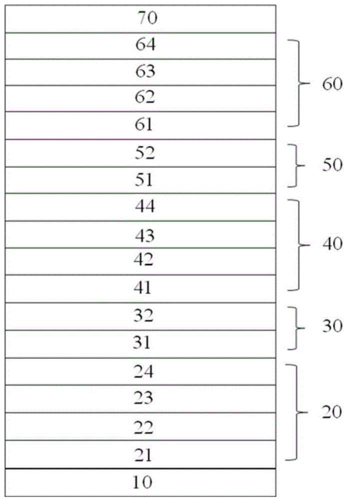
[0042] refer to figure 1 As shown, in the triple-junction cascaded solar cell structure of the present invention, the bottom, middle and top three cell layers are respectively GaAs 1-x-y N x Bi y 、In m Ga 1-m As 1-n N n 、Al p Ga 1-p Formed by As material, its forbidden band width is 0.94eV, 1.39eV, 1.93eV in turn.
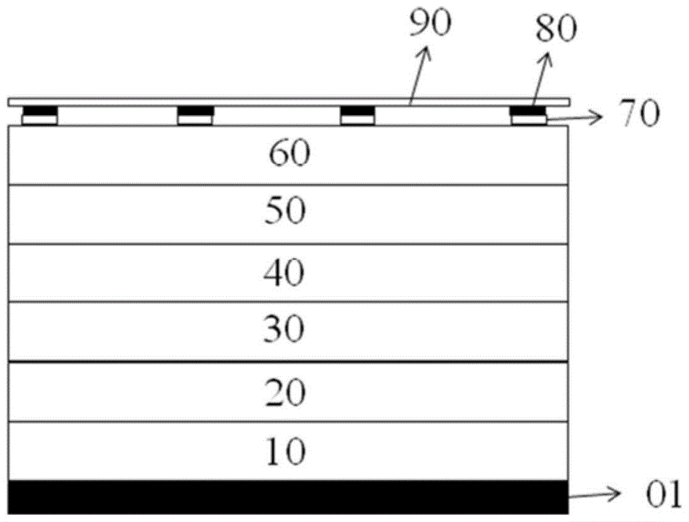
[0043] The specific structure is: GaAs grown sequentially on the GaAs substrate 10 1-x-y N x Bi y Bottom cell layer 20, first tunnel junction 30, In m Ga 1-m As 1-n N n Intermediate cell layer 40, second tunnel junction 50, Al p Ga 1-p As top cell layer 60 and GaAs contact layer 70 . combine figure 2 As shown, the solar cell further includes an upper ohmic electrode 80 , an anti-reflection film 90 disposed on the GaAs contact layer 70 in sequence, and a bottom electrode 01 formed at the bottom of the GaAs substrate 10 . Among them, the epitaxial layers of the triple-junction cascaded solar cells of the present invention are all prepared by metal...
Embodiment 2
[0058] The structure of the triple-junction cascaded solar cell of the present invention is the same as that of Embodiment 1. refer to figure 1 and figure 2 As shown, its solar cell structure includes bottom, middle, and top three cell layers, which are respectively In x Ga 1-x As 1-y N y 、In m Ga 1-m As 1-n N n 、Al p Ga 1-p Formed by As material, its forbidden band width is 0.94eV, 1.39eV, 1.93eV in turn.
[0059] The specific structure is: In grown sequentially on the GaAs substrate 10 x Ga 1-x As 1-y N y Bottom cell layer 20, first tunnel junction 30, In m Ga 1-m As 1-n N n Intermediate cell layer 40, second tunnel junction 50, Al p Ga 1-p As top cell layer 60 and GaAs contact layer 70 . combine figure 2 As shown, the solar cell also includes an upper ohmic electrode 80 , an anti-reflective film 90 sequentially disposed on the GaAs contact layer 70 , and a bottom electrode 01 formed at the bottom of the GaAs substrate 10 . Among them, the epitaxial ...
Embodiment 3
[0074] The structure of the triple-junction cascaded solar cell of the present invention is the same as that of Embodiment 1. refer to figure 1 and figure 2 As shown, in the triple-junction cascaded solar cell structure of the present invention, the bottom, middle and top three cell layers are respectively GaAs 1-x-y N x Bi y , B m Ga 1-m-n In n As, Al p Ga 1-p As material, the specific structure is: GaAs sequentially grown on the GaAs substrate 10 1-x-y N x Bi y Bottom cell layer 20, first tunnel junction 30, B m Ga 1-m-n In n As intermediate battery layer 40, second tunnel junction 50, Al p Ga 1-p As top cell layer 60 and GaAs contact layer 70 . combine figure 2 As shown, the solar cell also includes an upper ohmic electrode 80 , an anti-reflective film 90 sequentially disposed on the GaAs contact layer 70 , and a bottom electrode 01 formed at the bottom of the GaAs substrate 10 . Among them, the epitaxial layers of the triple-junction cascaded solar cell...
PUM
 Abstract
Description
Claims
Application Information
 - Generate Ideas
- Intellectual Property
- Life Sciences
- Materials
- Tech Scout
- Unparalleled Data Quality
- Higher Quality Content
- 60% Fewer Hallucinations
Browse by: Latest US Patents, China's latest patents, Technical Efficacy Thesaurus, Application Domain, Technology Topic, Popular Technical Reports.
© 2025 PatSnap. All rights reserved.Legal|Privacy policy|Modern Slavery Act Transparency Statement|Sitemap|About US| Contact US: help@patsnap.com


