


Quick Research
Generate reliable direction feasibility study reports for your R&D in just a few steps.

Technical Q&A
Discover and master advanced knowledge NOW. Basics, ideas, possibilities, all at once.

Find Solutions
As an expert in R&D theories, this can generate solutions to your technical problems instantly.

Evaluate Feasibility
Analyze your overall solution with one click, know your potential R&D risks in advance.

Monitor Landscape
Get weekly tech updates, stay abreast of the latest tech innovations and key insights.
DA (Digital to Analog) converter
A technology of digital-to-analog converter and operational amplifier, applied in the direction of analog/digital conversion, code conversion, instruments, etc., can solve the problem that the coupling of the switch control signal to the output terminal needs to be reduced, and the effect is not obvious, so as to reduce the coupling and increase the power. Consumption, improve the effect of SFDR
- Summary
- Abstract
- Description
- Claims
- Application Information
AI Technical Summary
Problems solved by technology
Method used
Image

Examples
Embodiment 1
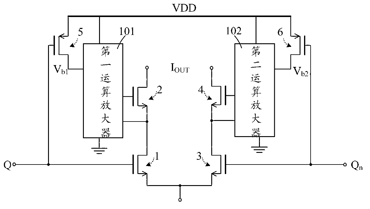
[0049] This embodiment provides a digital-to-analog converter, the structure of the switch unit is: an operational amplifier is respectively arranged on both sides of the four MOS transistors connected in pairs to form a cascode structure, and each operational amplifier is connected A MOS tube that controls its on or off. Specifically, such as figure 1 Shown is the basic structural diagram of the switch unit of the digital-to-analog converter provided by the present invention, the switch unit includes: a first MOS transistor 1, a second MOS transistor 2, a third MOS transistor 3, a fourth MOS transistor 4, The fifth MOS transistor 5 and the sixth MOS transistor 6, the first operational amplifier 101 and the second operational amplifier 102, wherein:
[0050] The drain of the first MOS transistor 1 is connected to the source of the second MOS transistor 2 to form a cascode structure, and the drain of the third MOS transistor 3 is connected to the source of the fourth MOS trans...
Embodiment 2
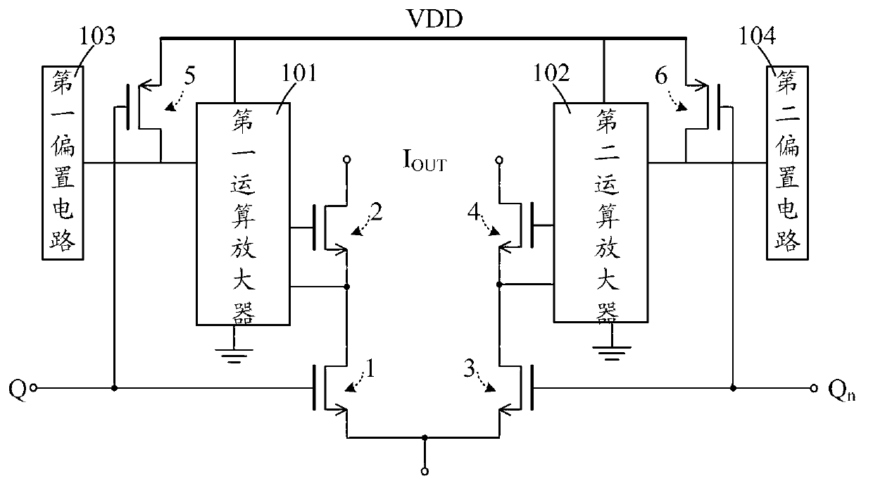
[0085] Based on the first embodiment, this embodiment provides specific implementations of the first operational amplifier 101 , the second operational amplifier 102 , the first bias circuit 103 and the fourth bias circuit 104 .
[0086] Such as Figure 5 Shown is a specific structure of the switch unit of the digital-to-analog converter provided in this embodiment. The first operational amplifier 201 and the second operational amplifier 202 are single-stage operational amplifiers, respectively composed of two MOS transistors.
[0087]Specifically, the first operational amplifier 201 includes: a seventh MOS transistor 7 and an eighth MOS transistor 8, the drain of the seventh MOS transistor 7 is connected to the drain of the eighth MOS transistor 8; The first input end of the amplifier 201 is the gate of the seventh MOS transistor 7, the second input end of the first operational amplifier 201 is the drain electrode of the eighth MOS transistor 8, and the first operational ampl...
Embodiment 3
[0098] Based on Embodiment 1, this embodiment provides another specific implementation of the first operational amplifier and the second operational amplifier. Compared with the switching unit in Embodiment 2, the output impedance of the switching unit in this embodiment is further improved by one. about times.
[0099] Such as Image 6 As shown, the first operational amplifier 301 of the switch unit includes: an eleventh MOS transistor 11, a twelfth MOS transistor 12, a thirteenth MOS transistor 13, and a fourteenth MOS transistor 14. The eleventh MOS transistor 11 The drain is connected to the source of the twelfth MOS transistor 12, the drain of the twelfth MOS transistor 12 is connected to the drain of the thirteenth MOS transistor 13, and the source of the thirteenth MOS transistor 13 Connect the drain of the fourteenth MOS transistor 14; the first input terminal of the first operational amplifier 301 is the gate of the twelfth MOS transistor 12, and the second input ter...
PUM
 Abstract
Description
Claims
Application Information
 - R&D Engineer
- R&D Manager
- IP Professional
- Industry Leading Data Capabilities
- Powerful AI technology
- Patent DNA Extraction
Browse by: Latest US Patents, China's latest patents, Technical Efficacy Thesaurus, Application Domain, Technology Topic, Popular Technical Reports.
© 2024 PatSnap. All rights reserved.Legal|Privacy policy|Modern Slavery Act Transparency Statement|Sitemap|About US| Contact US: help@patsnap.com