Eureka AIR delivers breakthrough ideas for toughest innovation challenges, trusted by R&D personnel around the world.

Backplanes for electro-optic displays

a backplane and electrooptic technology, applied in the direction of optics, electrostatic/electro-adhesion relays, instruments, etc., can solve the problems of inability to meet the needs of the user, inadequate service life of these displays, and inability to achieve widespread us

Active Publication Date: 2008-07-10
E INK CORPORATION
View PDF99 Cites 78 Cited by
  • Summary
  • Abstract
  • Description
  • Claims
  • Application Information

AI Technical Summary

Benefits of technology

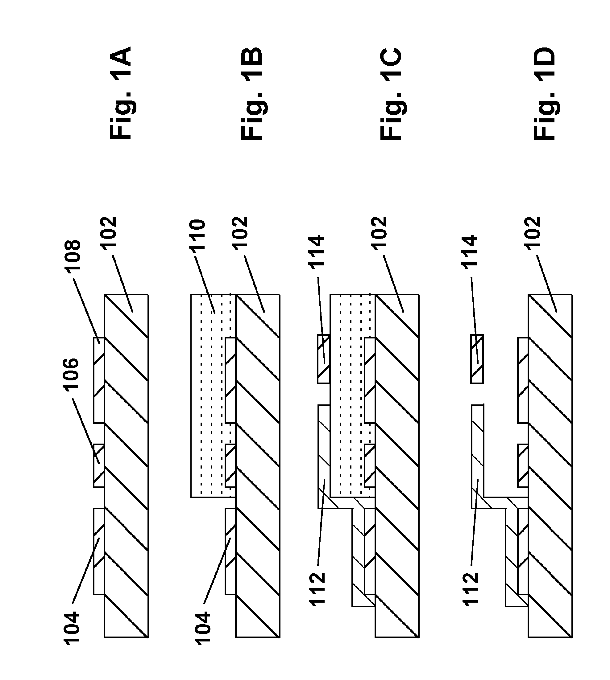
[0069]The MEMS-based backplane of the present invention provides several important technical advantages. A MEMS switch has a low impedance in its “on” state and a very high impedance in its “off” state, thus providing an excellent on / off ratio and thus avoiding problems associated with leakage currents passing through other types of non-linear elements. As discussed above with reference to FIGS. 1A-1D, a MEMS switch can be fabricated in a simple process using only three or four masks and not requiring any high temperature processing steps. Thus, the process can be used on low cost flexible substrates, for example poly(ethylene terephthalate) films. Furthermore, the MEMS fabrication process described above is less susceptible to environmental contamination during processing than are processes for fabricating backplanes based on thin film transistors or diodes, which tends to reduce the cost of the clean room facilities needed. Also, the fabrication process for a MEMS-based backplane can make use of some coarse patterning steps.

Problems solved by technology

Nevertheless, problems with the long-term image quality of these displays have prevented their widespread usage.
For example, particles that make up electrophoretic displays tend to settle, resulting in inadequate service-life for these displays.
However, in a high resolution display, for example a VGA (640×480) display, this architecture becomes impracticable because of the enormous number of electrical leads required.
However, the present state of such techniques is not optimized for fabrication of backplanes.

Method used


Image

  • Backplanes for electro-optic displays
  • Backplanes for electro-optic displays
  • Backplanes for electro-optic displays

Examples


Embodiment Construction

[0058]As already indicated, this invention has several different aspects, each providing an improvement in backplanes for electro-optic displays; some aspects of the invention may also be useful in other applications. Hereinafter, the major aspects of the present invention will be described separately, but it should be understood that more than one aspect of the invention may be used in the fabrication of a single backplane or other electronic component. For example, a MEMS backplane of the present invention may be fabricated using an embossing method of the present invention.

[0059]Part A: MEMS Backplane

[0060]As already discussed, prior art active matrix displays require non-linear (transistor or diode) switching elements at each pixel. Currently non-linear transistor elements may be fabricated from amorphous silicon, polysilicon and organic semiconductors. Diode switching elements include metal insulator metal (MIM), metal semiconductor insulator (MSI), Schottky, and NIN diodes. Th...


PUM

PropertyMeasurementUnit
thicknessaaaaaaaaaa
thicknessaaaaaaaaaa
thicknessaaaaaaaaaa

Abstract

A backplane for an electro-optic display comprises a pixel electrode (104), a voltage supply line (C) arranged to supply a voltage to the pixel electrode (104), and a micromechanical switch (106, 112) disposed between the voltage supply line (C) and the pixel electrode (104), the micromechanical switch (106, 112) having an open state, in which the voltage supply line (C) is not electrically connected to the pixel electrode (104), and a closed state, in which the voltage supply line (C) is electrically connected to the pixel electrode (104).

Description

REFERENCE TO RELATED APPLICATIONS[0001]This application is a divisional of copending application Ser. No. 10 / 707,466, filed Dec. 16, 2003 (Publication No. 2004 / 0196215), which itself claims benefit of Application Ser. No. 60 / 319,786, filed Dec. 16, 2002.[0002]This application is also related to copending Application Ser. No. 60 / 375,508, filed Apr. 24, 2002, and copending application Ser. No. 10 / 249,618, filed Apr. 24, 2003 (now U.S. Pat. No. 7,116,318. The entire disclosures of the aforementioned applications, and of all U.S. patents and published and copending applications referred to below, are also herein incorporated by reference.BACKGROUND OF INVENTION[0003]This invention relates to backplanes for electro-optic displays, and to processes for the formation of such backplanes. The backplanes of the present invention are especially, but not exclusively, intended for use with particle-based electrophoretic displays in which one or more types of electrically charged particles are su...

Claims


Application Information

Patent Timeline
Patent Type & Authority Applications(United States)
IPC IPC(8): G09G3/34G02B26/00G02F1/1362G02F1/167H01H59/00
CPCG02F1/1362H01H59/0009G02F1/167G02F1/136213G02F1/1365H01H59/00
Inventor DUTHALER, GREGG M.ZEHNER, ROBERT W.HONEYMAN, CHARLES H.DENIS, KEVIN L.KING, MATTHEW A.WANG, JIANNA
Owner E INK CORPORATION
Why Eureka
Eureka Blog
Learn More