A kind of testing device and testing method of TFT substrate
A technology for testing devices and testing methods, which is applied in the directions of measuring devices, measuring electricity, and measuring electrical variables, etc., which can solve the problems of frequent replacement of test frames, etc., and achieve the goal of avoiding storage space and capital occupation, preventing probe damage, and avoiding collisions Effect
- Summary
- Abstract
- Description
- Claims
- Application Information
AI Technical Summary
Problems solved by technology
Method used
Image

Examples
Embodiment 1
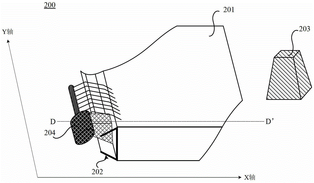
[0073] Such as figure 2 As shown, the TFT substrate testing device 200 of this embodiment includes: a stage 201, a sliding structure 202 provided on at least one side of the stage 201, a detection unit 203 located above the stage 201, and at least one probe Needle unit 204.
[0074] The sliding structure, the probe unit and the detection unit will be described in detail below in order.
[0075] Sliding structure
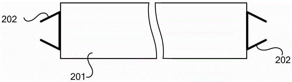
[0076] Such as image 3 As shown, the sliding structure 202 is a sliding rail arranged on the side of the carrier 201 and parallel to the side. In this embodiment, the sliding structure 202 is respectively arranged on two sides of the carrier 201. It can be understood that in order to adapt to TFT substrates of more specifications, sliding structures 202 may also be provided on two or more sides or all sides of the carrier 201. Of course, as long as the test of the TFT substrate to be tested can be completed, the sliding structure 202 can also be provided on only one si...
Embodiment 2
[0098] The difference between this embodiment and the first embodiment is that the sliding structure 202 is a sliding groove opened on the side of the carrier 201 and parallel to the side. Such as Picture 9 As shown, the sliding structure 202 is arranged on two sides of the carrier 201 respectively. It can be understood that, in order to adapt to TFT substrates of more specifications, sliding structures 202 may also be provided on all sides of the carrier 201. Of course, as long as the test of the TFT substrate to be tested is completed, the sliding structure 202 can also be provided on only one side of the carrier 201.
Embodiment 3
[0100] Such as figure 2 As shown, in the first embodiment, through the sliding structure 202, the probe 205 can be along the length direction of the sliding structure 202 ( figure 2 In the Y-axis direction) freely sliding, but not along the width direction of the sliding structure 202 ( figure 2 If the signal access point of the TFT substrate changes in the width direction of the sliding structure 202, the test device for the TFT substrate cannot be used for testing. For this reason, in this embodiment, the cross-section of the sliding member 206 is designed to be rectangular to ensure that the probe 205 can also have a certain range of movement along the width direction of the sliding structure 202 (the direction perpendicular to the length direction).
[0101] Such as Picture 10 As shown, by controlling the embedded length of the sliding member 206 in the sliding structure 202, the sliding member 206 can be moved in a small range along the width direction of the sliding struc...
PUM
 Abstract
Description
Claims
Application Information
 - R&D
- Intellectual Property
- Life Sciences
- Materials
- Tech Scout
- Unparalleled Data Quality
- Higher Quality Content
- 60% Fewer Hallucinations
Browse by: Latest US Patents, China's latest patents, Technical Efficacy Thesaurus, Application Domain, Technology Topic, Popular Technical Reports.
© 2025 PatSnap. All rights reserved.Legal|Privacy policy|Modern Slavery Act Transparency Statement|Sitemap|About US| Contact US: help@patsnap.com