
Packaging method of organic electronic device

A technology of organic electronic devices and packaging methods, applied in the direction of electric solid devices, electrical components, semiconductor devices, etc., can solve the problems that rigid packaging cannot meet the packaging requirements of flexible devices, and achieve the goal of improving service life, reducing costs, and reducing thermal damage Effect

Inactive Publication Date: 2016-02-03
INST OF MICROELECTRONICS CHINESE ACAD OF SCI
View PDF5 Cites 0 Cited by
  • Summary
  • Abstract
  • Description
  • Claims
  • Application Information

AI Technical Summary

Problems solved by technology

[0005] The traditional rigid OLED and OPV device packaging is generally used in the glove box to cover the device with epoxy resin cured glass and other packaging covers, and combined with the use of dry film packaging, but the rigid packaging cannot meet the packaging requirements of flexible devices, and the flexible plastic substrate itself The water oxygen permeability is also higher than 10-5g / m 2 / day, which requires water and oxygen barrier isolation for flexible substrates

Method used


Image

  • Packaging method of organic electronic device

Examples


Embodiment Construction

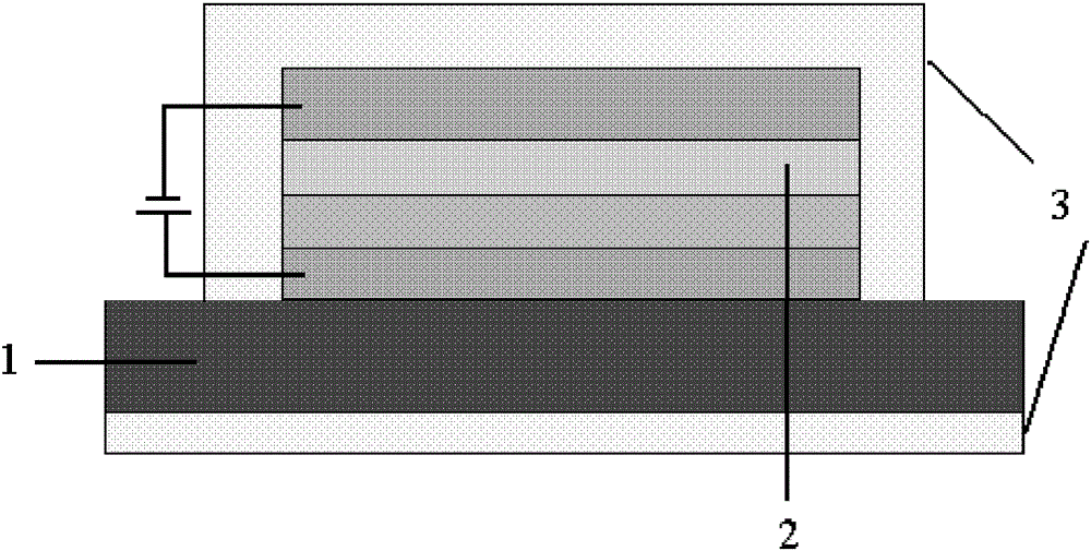
[0021] Such as figure 1 As shown, the packaging method for organic electronic devices provided by the present invention is divided into two steps: a pre-process and a post-process.

[0022] The pre-process is that before the organic electronic device 2 is fabricated, a multilayer composite film 3 is first deposited on the back of the substrate 1 material. A plasma enhanced chemical vapor deposition method (hereinafter referred to as a PECVD method) is used to deposit a multilayer composite film 3. The multilayer composite film 3 is composed of several stacked layers of alternating organic layers and inorganic layers. The organic layer is made of organic polymers, including: parylene, polypropylene, polyacrylate or silicone cross-linked polymer SiO x C y H z . It is used to isolate water and oxygen; the inorganic layer is an inorganic substance, which is used to increase flexibility, bend and prevent fracture. The inorganic layer is made of inorganic materials, including: SiN x...


PUM


Abstract

Disclosed is a packaging method for organic electronic devices, which includes: depositing a multi-layer composite film on the back of a substrate material before making the electronic device; and depositing a multi-layer composite film on the surface of the organic electronic device after the electronic device is made. The invention provides a packaging method for organic electronic devices, which adopts a chip-level packaging method and integrates the packaging process into the device manufacturing process, replacing the previous method of first manufacturing the device on the wafer and then packaging it separately. The benefit of this is to improve efficiency and reduce costs. At the same time, the invention innovatively adopts organic / inorganic composite multi-layer film packaging, which can not only isolate water and oxygen, thereby greatly improving the service life of organic electronic devices, but also achieving flexibility. Encapsulation, retaining the foldable and bendable properties of organic electronic devices to the greatest extent. Finally, this invention can achieve low-temperature film formation below 120°C, reducing thermal damage to devices and plastic substrates.

Description

Technical field [0001] The present invention relates to the field of electronic packaging, in particular to a packaging method for organic electronic devices. Background technique [0002] Organic optoelectronic devices have developed rapidly in the past two decades, especially organic light-emitting diodes (OLED), which have a series of advantages such as high luminous efficiency, low working voltage, lightness and flexibility, and their related technologies and industries have received extensive attention. At present, the annual output value of OLED displays exceeds one billion U.S. dollars, and the products involve TVs, MP3s, mobile phones, car audio, etc. OSRAM, GE, Philips and other traditional global lighting giants have invested heavily in the OLED lighting field and began to launch related products in 2009. According to the market analysis report of professional organization NanoMarkets, the OLED display and lighting market will reach 10.9 billion US dollars in 2012. Rea...

Claims


Application Information

Patent Timeline
Patent Type & Authority Patents(China)
IPC IPC(8): H01L51/00H10K99/00
Inventor 吴茹菲刘键
Owner INST OF MICROELECTRONICS CHINESE ACAD OF SCI
Learn More