Resistor substrate and method for manufacturing same
A technology of resistance substrate and manufacturing method, applied in resistance manufacturing, resistors, resistor parts and other directions, can solve the problems of poor yield of resistance substrate 100, poor micro-miniature linear characteristics, easy generation of static electricity, etc., and achieve linear characteristics. Optimum, miniaturization, and the effect of reducing static electricity
- Summary
- Abstract
- Description
- Claims
- Application Information
AI Technical Summary
Problems solved by technology
Method used
Image
Examples
no. 1 Embodiment approach ]
[0093] Hereinafter, the resistance substrate 1 in the first embodiment will be described.
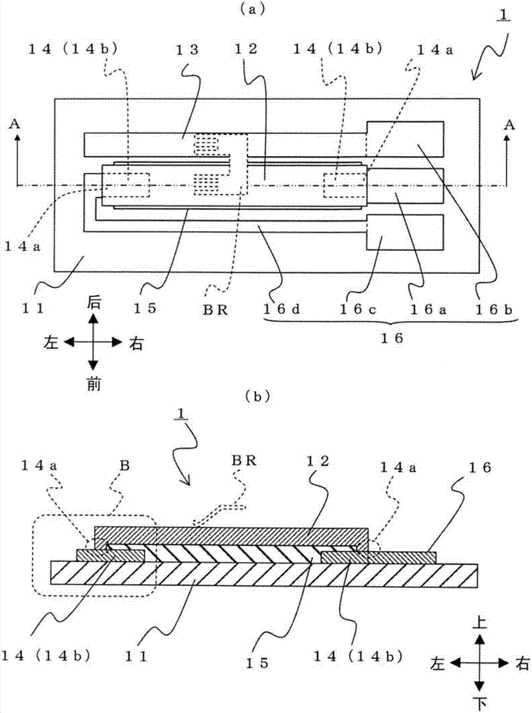
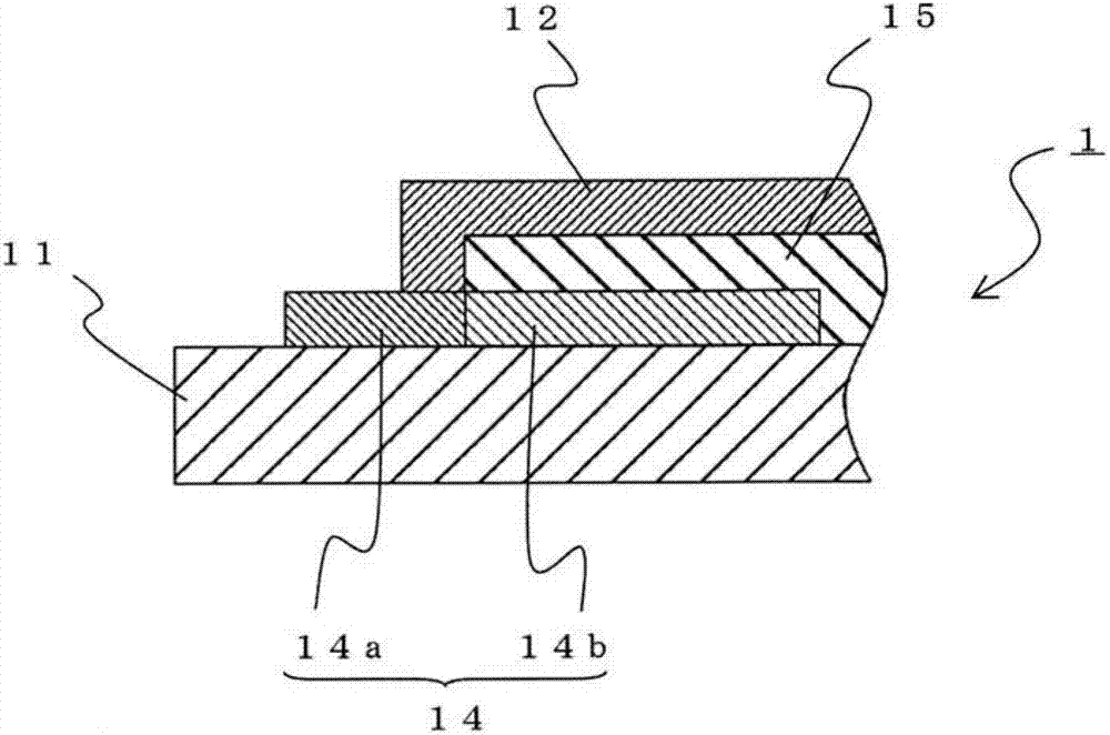
[0094] First, use Figure 1 to Figure 2 The configuration of the resistor substrate 1 in this embodiment will be described. figure 1 is a diagram showing the structure of the resistor substrate 1, figure 1 (a) is a figure which shows the resistance board|substrate 1 from the upper side, figure 1 (b) means figure 1 (a) Diagram of section A-A shown. figure 2 yes figure 1 (b) Enlarged view of part B shown.
[0095] Such as figure 1 (a) and figure 1 As shown in (b), the resistor substrate 1 separates and arranges a resistor pattern 12 and a current collector pattern 13 on which a conductive slider BR slides on an insulating insulating substrate 11 and juxtaposes them. A pair of conductive electrode patterns 14 are respectively formed at both ends. In addition, connecting portions 16 are formed on the current collector pattern 13 and the pair of electrode patterns 14 so as t...
no. 2 Embodiment approach ]
[0148] Below, use Figure 4 The resistance substrate 2 in the second embodiment will be described.
[0149] Including the manufacturing process, the resistor substrate 2 is the same resistor substrate as the resistor substrate 1 of the first embodiment, but the sliding region of the slider BR is different.
[0150] In the first embodiment, the resistor pattern 12 located on the extended portion 14b is used as a non-sliding area where the slider BR does not slide, and the Figure 4 The shown range S1 is the sliding area of the slider BR, but in the second embodiment, the resistor pattern 12 located on the extended portion 14b is included in the sliding area of the slider BR, and the Figure 4 The range S2 shown serves as the sliding area of the slider BR.
[0151] Hereinafter, effects brought about by employing this embodiment will be described.
[0152] In the resistor substrate 2 of the present embodiment, the resistor pattern 12 located on the extended portion 14b i...
PUM
 Abstract
Description
Claims
Application Information
 - R&D
- Intellectual Property
- Life Sciences
- Materials
- Tech Scout
- Unparalleled Data Quality
- Higher Quality Content
- 60% Fewer Hallucinations
Browse by: Latest US Patents, China's latest patents, Technical Efficacy Thesaurus, Application Domain, Technology Topic, Popular Technical Reports.
© 2025 PatSnap. All rights reserved.Legal|Privacy policy|Modern Slavery Act Transparency Statement|Sitemap|About US| Contact US: help@patsnap.com


