An enhanced flash chip and a chip packaging method
A chip packaging and enhanced technology, applied in multi-program devices, instruments, circuits, etc., can solve the problems of long design cycle, high design cost, and high design complexity, so as to improve yield, avoid cross problems, and reduce process effect of complexity
- Summary
- Abstract
- Description
- Claims
- Application Information
AI Technical Summary
Problems solved by technology
Method used
Image

Examples
Embodiment 1
[0067] Embodiment 1 of the present invention provides an enhanced Flash chip, and the chip may include: FLASH and RPMC packaged together.
[0068] In the embodiment of the present invention, the FLASH and the RPMC may be independent chips. FLASH can choose different capacities to meet the needs of different systems. This FLASH can reuse the designed FLASH chip, so it does not need to be redesigned, which greatly reduces the development cycle; RPMC has the function of response protection monotonic counting, and can also be used alone .
[0069] In the enhanced Flash chip proposed by the embodiment of the present invention, the FLASH and the RPMC may respectively include independent controllers. For commands sent from outside, FLASH and RPMC will control FLASH and RPMC to receive and decode them respectively through their independent controllers, and perform corresponding operations when the decoding is successful.
[0070] In addition, FLASH and RPMC can have the same IO pins...
Embodiment 2
[0082] In the following, the enhanced Flash chip will be introduced in detail through Embodiment 2 of the present invention.
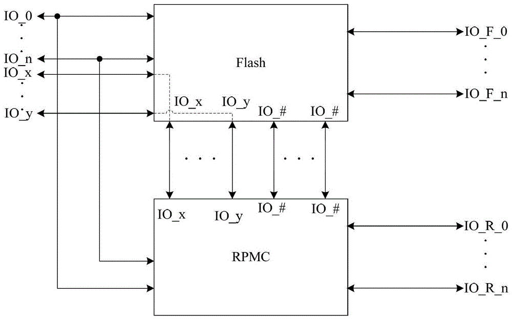
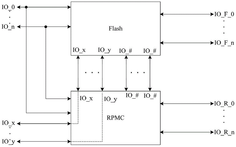
[0083] refer to Figure 1-a , Figure 1-b , which shows a schematic diagram of logical connections of an enhanced Flash chip according to Embodiment 2 of the present invention.
[0084] from Figure 1-a , Figure 1-b It can be seen that the enhanced Flash chip described in the embodiment of the present invention may include FLASH and RPMC packaged together.
[0085] Among them, both FLASH and RPMC include multiple pins respectively, and the same IO pins in RPMC and FLASH can be connected to the same set of external shared pins, and the commands sent externally will be received by RPMC and FLASH at the same time, RPMC and FLASH FLASH can respond accordingly; FLASH and RPMC each also include a first internal IO pin and a second internal IO pin, and FASH and / or RPMC connect the first IO internal pin to the corresponding RPMC and RPMC through the set P...
Embodiment 3
[0157] Next, the specific packaging method of the above chip will be introduced through the third embodiment of the present invention.
[0158] refer to image 3 , which shows a flow chart of a chip packaging method described in Embodiment 3 of the present invention, the packaging method may include:
[0159] Step 300, place the FLASH that needs to be packaged and the response protection monotonic counter RPMC on the chip carrier, the FLASH and the RPMC are independent of each other.
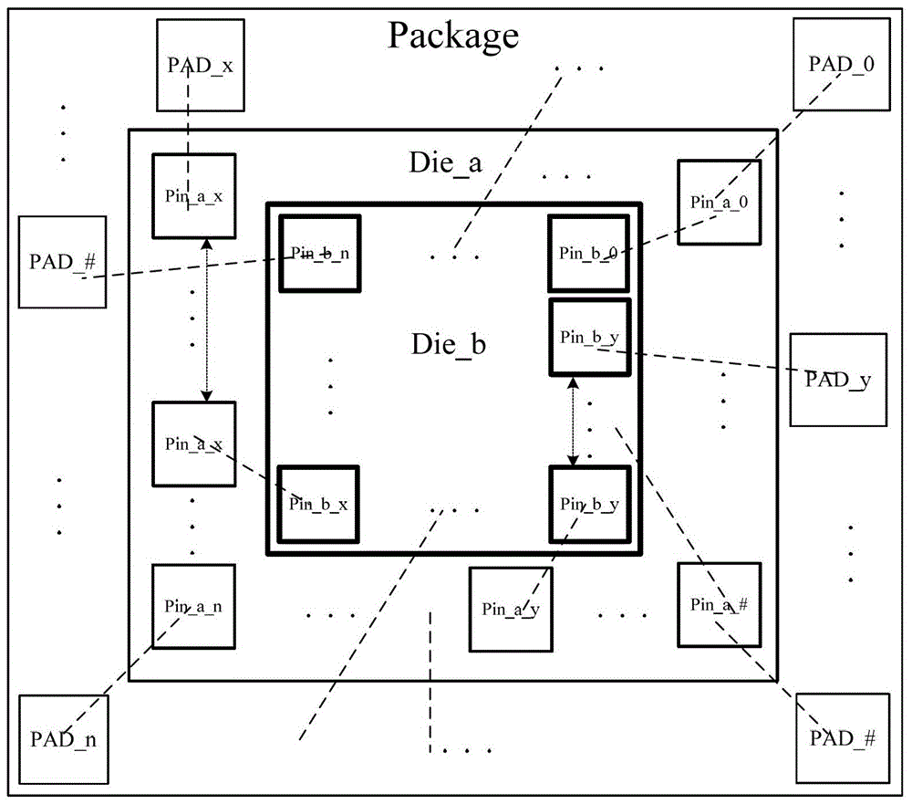
[0160] In the embodiment of the present invention, the FLASH and the RPMC are packaged together to obtain an enhanced Flash chip with RPMC function, and the FLASH and the RPMC in the chip are independent of each other.
[0161] First, the FLASH and RPMC that need to be packaged can be placed on the chip carrier, and the chip carrier described in the embodiment of the present invention can correspond to figure 2 in the Package.
[0162] Preferably, this step 300 may include: placing the FLASH ...
PUM
 Abstract
Description
Claims
Application Information
 - Generate Ideas
- Intellectual Property
- Life Sciences
- Materials
- Tech Scout
- Unparalleled Data Quality
- Higher Quality Content
- 60% Fewer Hallucinations
Browse by: Latest US Patents, China's latest patents, Technical Efficacy Thesaurus, Application Domain, Technology Topic, Popular Technical Reports.
© 2025 PatSnap. All rights reserved.Legal|Privacy policy|Modern Slavery Act Transparency Statement|Sitemap|About US| Contact US: help@patsnap.com