Gradient band gap nano-silicon thin film and graded band gap nano-silicon thin film solar cell

A nano-silicon thin film and solar cell technology, which is applied in circuits, photovoltaic power generation, electrical components, etc., can solve the problems of low open-circuit voltage and fill factor, large light-induced attenuation, and low conversion efficiency of nano-silicon solar cells, so as to avoid interface problems. effect, increased short-circuit current, and low manufacturing cost

Active Publication Date: 2017-02-08
晶怿能源科技(上海)有限公司
View PDF7 Cites 0 Cited by
  • Summary
  • Abstract
  • Description
  • Claims
  • Application Information

AI Technical Summary

Problems solved by technology

[0003] The purpose of the present invention is to solve the problems of low conversion efficiency, large light-induced attenuation and low open-circuit voltage and fill factor of traditional silicon thin-film solar cells, and to provide a new graded bandgap nano-silicon thin-film material and its preparation Gradient Bandgap Nano-Silicon Thin Film Solar Cells

Method used


Image

  • Gradient band gap nano-silicon thin film and graded band gap nano-silicon thin film solar cell
  • Gradient band gap nano-silicon thin film and graded band gap nano-silicon thin film solar cell
  • Gradient band gap nano-silicon thin film and graded band gap nano-silicon thin film solar cell

Examples


Embodiment Construction

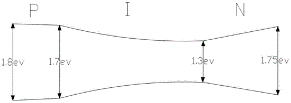
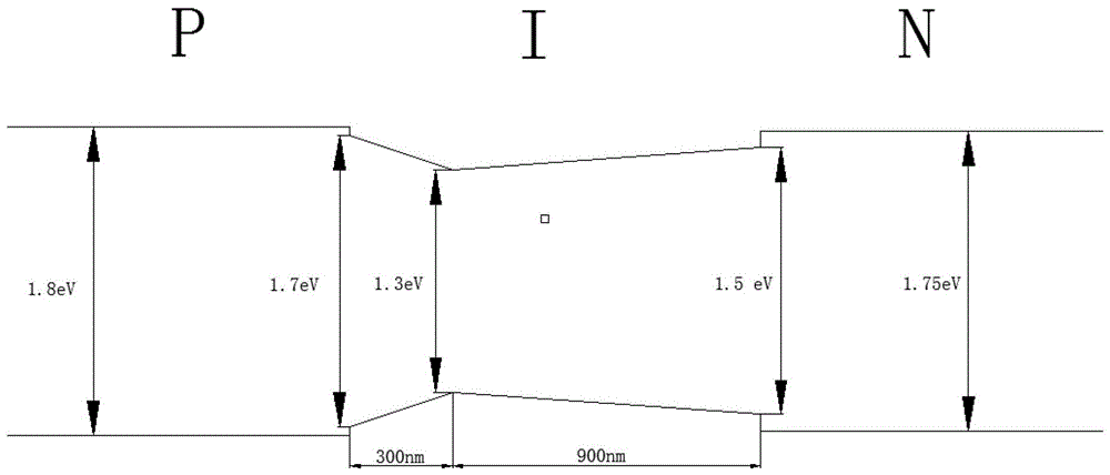
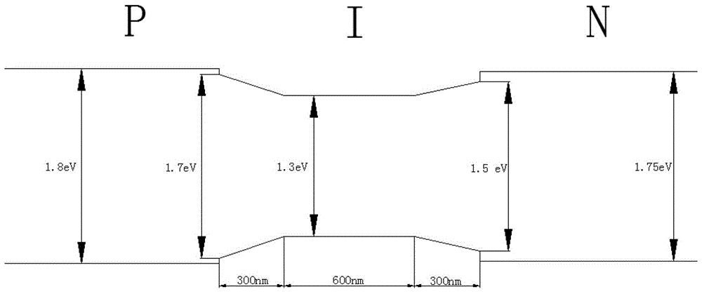
[0026] The graded bandgap nano-silicon thin film material in this specific embodiment is a mixed-phase material composed of amorphous silicon, crystal grains and grain boundaries. The band gap of the selected crystalline silicon is 1.12eV, and that of amorphous silicon is 1.75eV; the crystallization rate of nano-silicon thin film (the ratio of crystal phase to amorphous phase) ) ranges from 40% to 70%; by controlling the crystallization rate to change within the aforementioned range, the bandgap of the nano-silicon thin film with graded bandgap is 1.3eV~1.5eV. The method of controlling the crystallization rate includes adjusting the core preparation parameters of the nano-silicon thin film, such as the concentration of silane (SC), the level of the preparation power and the level of the preparation pressure, etc.

[0027] The graded bandgap has multiple structures, and the present invention proposes four schemes, the first such as figure 1 As shown in , a "C" type graded stru...


PUM

PropertyMeasurementUnit
band gapaaaaaaaaaa
band gapaaaaaaaaaa
band gapaaaaaaaaaa

Abstract

The invention discloses a graded bandgap nano-silicon film and a graded bandgap nano-silicon film solar cell. The graded bandgap nano-silicon film is a mixed phase material consisting of noncrystalline silicon, crystal grains and a crystal boundary, wherein a bandgap of crystalline silicon is 1.12eV; a bandgap of the noncrystalline silicon is 1.75eV; a crystalline fraction scope of the device-level nano-silicon film is 40-70%; and a bandgap of the graded bandgap nano-silicon film is 1.3-1.5eV. The graded bandgap nano-silicon film is used for an I layer (namely a light absorption layer) of the nano-silicon cell, absorbs sunlight energy in different wavebands sufficiently, improves transmission of photoproduction holes, and therefore can effectively improve the photoelectric conversion efficiency of the cell; in addition, a graded light absorption layer structure solves the problem that the open circuit voltage of the nano-silicon solar cell is lower; the graded structure allows bandgap differences between the I layer and a P layer and between the I layer and an N layer to be less; the problem of bandgap mismatch of P / I and I / N interfaces is solved to a greater extent; the interfacial effect of a heterojunction is avoided; the photoinduced degradation effect is reduced; and the cost is lowered.

Description

technical field [0001] The invention relates to the field of silicon thin-film solar cells, in particular to a nano-silicon thin film with a gradient band gap and a solar cell made of the nano-silicon thin film. Background technique [0002] Silicon thin-film solar cells have the advantages of less raw material consumption, easy large-area continuous production, and less pollution in the preparation process; they are an important development direction of photovoltaic cells. Amorphous silicon cells have a light-induced degradation effect, which limits its development. Nano-silicon (microcrystalline silicon) solar cells have good material order and basically no degradation, and can be combined with amorphous silicon cells to prepare stacked cells to improve Efficiency and cost reduction. Existing nano-silicon thin-film solar cells cannot fully absorb solar light energy in different bands, have low power conversion efficiency, large light-induced attenuation, and low open-circ...

Claims


Application Information

Patent Timeline
Patent Type & Authority Patents(China)
IPC IPC(8): H01L31/076H01L31/0352
CPCY02E10/548
Inventor 于化丛
Owner 晶怿能源科技(上海)有限公司
Why Eureka
Try Eureka