Full-page printed wiring board
A technology for printed circuit boards and circuit boards, which is applied in the directions of printed circuit components and structural connections of printed circuits.
- Summary
- Abstract
- Description
- Claims
- Application Information
AI Technical Summary
Problems solved by technology
Method used
Image

Examples
Embodiment Construction
[0009] The present invention will be further described below in conjunction with specific examples.
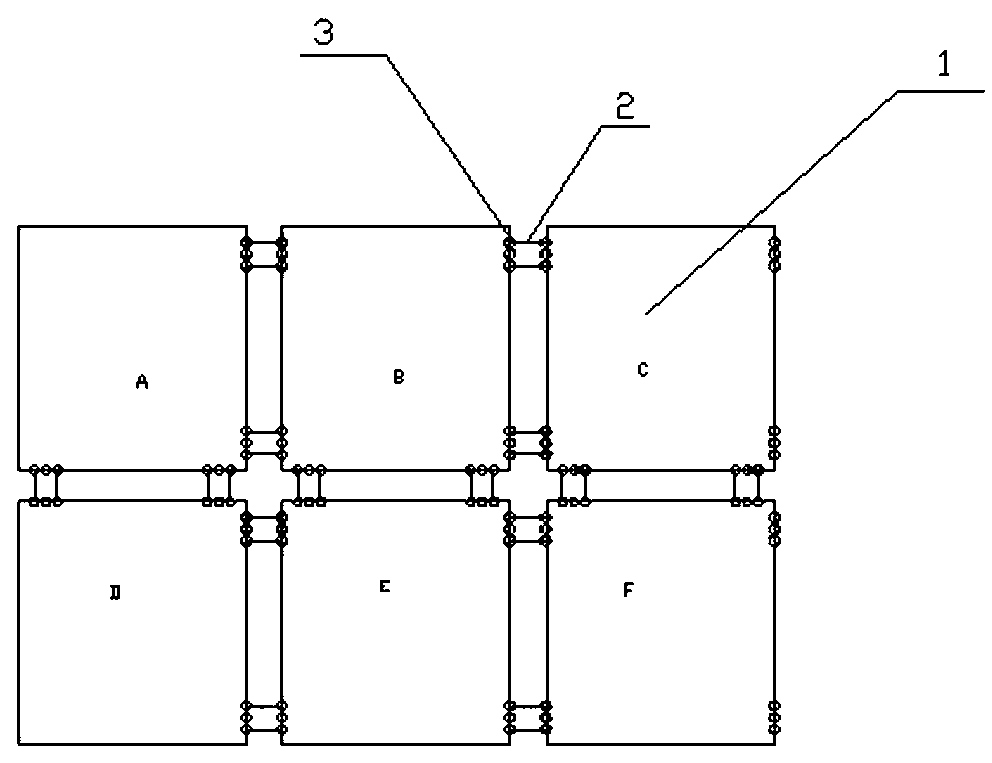
[0010] refer to figure 1 Each circuit board 1 of the full-page printed circuit board is connected through a connection position 2, and the connection position 2 and the circuit board 1 are connected through a stamp hole 3. In this way, the purpose of easily dividing the boards between each circuit board is achieved through the stamp holes, which is fast and convenient, and reduces the process.
PUM
 Abstract
Description
Claims
Application Information
 - R&D
- Intellectual Property
- Life Sciences
- Materials
- Tech Scout
- Unparalleled Data Quality
- Higher Quality Content
- 60% Fewer Hallucinations
Browse by: Latest US Patents, China's latest patents, Technical Efficacy Thesaurus, Application Domain, Technology Topic, Popular Technical Reports.
© 2025 PatSnap. All rights reserved.Legal|Privacy policy|Modern Slavery Act Transparency Statement|Sitemap|About US| Contact US: help@patsnap.com